This thread has been locked.

If you have a related question, please click the "Ask a related question" button in the top right corner. The newly created question will be automatically linked to this question.

ADS1262: Inquire whether the digital filter configuration problem

Part Number: ADS1262

1. Configure the negative voltage pins of the ADS126 acquisition terminal as AINCOM:GND, and configure the positive voltage pins as AIN1 and AIN0 respectively. The voltage can be stably measured as -2.499V and 2.499V.

2. Configure the negative voltage pin of ADS126 acquisition terminal as AINCOM:GND, and the positive voltage pin as AIN2. The measured data is shown in the following figure, with large deviation (the actual input waveform is relatively stable square wave).

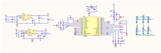
3. The specific configuration of ADS1262 is as follows:

Chop on, PGA on, PGA gain 1V/V, 1200 SPS, Sinc1 mode, full-scale Calibration Registers:0C75ba

4. Summary of problems:

(1) The voltage drift collected by the pin of the digital filter is very large, how to configure the register to solve it?

(2) How to accurately determine the gain coefficient and migration coefficient (for calibration)

  • Hi,

    Thanks for your query.

    I am not sure what this means:

    The voltage drift collected by the pin of the digital filter is very large, how to configure the register to solve it?

    The ADC digital filter does not have any pins associated with it, so I do not know how this could be contributing drift.

    How are you applying the signal to the ADC? Are you using a function generator? Is the output signal from the function generator (or whatever you are using) in any way connected to the ADC board, or is the output signal floating with respect to the ADC?

    To perform a gain calibration, you would first perform an offset calibration by shorting the input terminals together to a mid-supply voltage and taking several readings. You can then average these readings together to determine the average offset for that channel (it can be different on a channel-to-channel basis, depending on how your system is configured). This value can be stored in the ADC's OFCAL register, or in the MCU. Then, you would apply a close to full-scale signal to the inputs, take several readings, and average them together to determine the gain error. This error is assumed to be linear over input signal, and changes the slope of the ADC's transfer function. This can be stored in the ADC's FSCAL register or in the MCU.

    You can also reference our Precision Labs content for more information. Specifically, section 5 on Error Sources: https://training.ti.com/ti-precision-labs-adcs

    -Bryan

  • I turned on THE MCU CHOP on, according to the manual, the offset register should be invalid, so only one gain register is valid. When using the external DC power supply for calibration, 2.499V input was used, and multiple data were collected and averaged. After obtaining the gain coefficient, the full range could indeed be calibrated to 2.499V, but the voltage was adjusted to different gears. For example, 1V: the result is 1.2V, 2V: the result is 2.1V, not linear.

  • Any update for me?

  • Hi,

    Bryan is currently out of the office, so I will try to help.  I think you should back up a step and not try any calibration or chopping at this point.  Please send the configuration register settings as hex values and not descriptions of the settings.  Also, when you were connecting the square wave input, what was the measured signal (do you have oscilloscope shots)?  What is the frequency of the square wave signal?  Depending on the frequency used there could be considerable droop.

    Also, it is a good idea to check noise performance of the ADC with shorted inputs.  You should be able to match the noise as given in the datasheet for Sinc1 and 1200sps for a gain of 1.  The peak to peak noise is 17.755uV.  If you are seeing worse noise, then you need to make corrective actions.

    Best regards,

    Bob B