This thread has been locked.

If you have a related question, please click the "Ask a related question" button in the top right corner. The newly created question will be automatically linked to this question.

TSW14J10EVM: TSW14J10 and VC707 - ADC board selection

Part Number: TSW14J10EVM

Dear,

I have trouble in understanding how the TSW14J10 knows what FPGA it is connected to. As can be seen in the attached screenshot it identifies for me as connected to a Xilinx ZC706. However I want to use it with a Xilinx VC707. And at the moment I can also only see the ADC selection of the ZC706. How do I change this? Does this also mean the wrong bit/svf file is uploaded to the FPGA? 

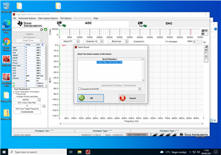
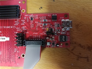
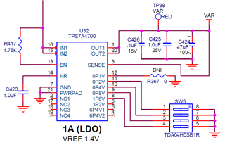
Besides that I was also wondering where SW5 dip switches are for? From another forum post I saw all the dip switches were to one way but for me that doesn't seem the case. Should I change this?

  • Hi Jan,

    It appears that HSDC Pro is recognizing the VC707 as a ZC706, likely due to incorrect firmware uploaded to the FPGA. I'll check with the team on this. In the meantime, which files are being used to program the VC707? Are these the files shown at the following path? C:\Program Files (x86)\Texas Instruments\High Speed Data Converter Pro\14J10VC707 Details\Firmware

    Regarding SW5, these dip switches are used to adjust the output voltage of the VAR net. Placing the switch to the ON position will increase the output voltage of U32 (by the amount listed for that pin in the snippet of the schematic below). The switch position shown in your image indicates the VAR voltage should read 1.8V. You can verify this by measuring voltage at the VAR test point (to the left of SW5). 


    Regards

  • Jan,

    If the ribbon cable is not connected properly and the VC707 is not powered up, the GUI will default to ZC706. Double check that the ribbon cable is connected properly as shown in the TSW14J10EVM User's Guide, figure 13.

    Regards,

    Jim