This thread has been locked.

If you have a related question, please click the "Ask a related question" button in the top right corner. The newly created question will be automatically linked to this question.

ADC3683: differential input impedance for simulating AAF and Glitch Filter

Part Number: ADC3683

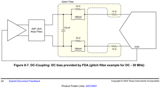
I do not really understand the function / the effect of the recommended Glitch Filter between AAF and ADC. The description in the ADC data sheet is not detailed enough for me. The EVM uses different values for the Glitch Filter than the ADC data sheet.

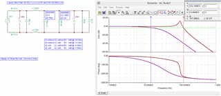
However, I have to design an AAF stage together with the Glitch Filter suitable to our requirements. The AC Transfer characteristic with that Glitch Filter design strongly depends from the input impedance of the ADC input.

Is there any description how to calculate the values for R, L and C’s of the Glitch Filter?

Is it sufficient, to use the ADC data sheet input impedance values 8kOhm and 7pF for the AC simulation of the filters?
Or depends the ADC input impedance from the sampling frequency?

Our requirements are: sampling frequency 62.5MHz, used analog bandwidth DC to 15MHz, Antialiasing & Glitch Filter Low pass cutoff at 15MHz (-3dB), stopband from 60MHz (<-50dB)

Thanks in advance.

  • Hello,

    Since the ADC3683's analog input is unbuffered, a "glitch filter" (placed as close as possible to the ADC analog input pins) is utilized to attenuate the glitch/kickback energy that is created when the sample/hold caps switch. This glitch energy is synchronous with the sample clock frequency (62.5 MHz clock rate = 62.5 MHz glitch energy seen on analog inputs), and should be filtered as much as possible to ensure that the glitch energy has settled as much as possible during the acquisition stage of the ADC as to not effect the final ADC measurement (hold stage).

    The EVM has a two pole ~30 MHz LPF glitch filter [The cap (red) and inductors (yellow) ] when driving the glitch filter with a 50 ohm source (utilizing the transformer/balun inputs). These two components can be adjusted (also resistance) to change the corner frequency (Fc) of the LPF/AAF. There are different software programs that may be helpful (like Nuhertz) for filter design. You can also use TINA spice simulator (free). There is a TINA reference design that may be helpful.

    If you intend to utilize an FDA to drive the analog inputs, the same rules apply for the glitch filter. Just ensure that the output resistors on the FDA are set accordingly with the filter design. If you look at the FDA output on the ADC3683EVM, we also include an AAF, as well as the glitch filter. These components are used to provide additional filtering for steeper roll off and allow for more filter design options.

    These two filters (20 MHZ LPF and the Glitch Filter) combine together to have an Fc of ~18 MHz, so this topology may be a good starting point for a 15 MHz Fc.

    Now to answer your questions = )

    • Is it sufficient, to use the ADC data sheet input impedance values 8kOhm and 7pF for the AC simulation of the filters?
      • Yes, this would be the correct values to simulate with. However, I would recommend utilizing the topology of the glitch filter shown in the datasheet and on the EVM.
    • Or depends the ADC input impedance from the sampling frequency?
      • The input impedance will change with regard to the analog input frequency, and not with the sampling frequency.

    Best Regards,

    Dan

  • Thanks dBrock for the explanations.

    I have simulated the LP and glitch filter from the EVM.

    Case [1] (the red curve) is for the values given in the schematic (like your second picture). The -3dB point is at 122 MHz, far away from the stated 18 MHz.
    Case [3] (the violet curve) is much closer. But this is not what you mean, is it?

    Or have I made a mistake with my simulation?
    The values for the ADC input impedance Ri and Ci are quite important for the behavior of the whole filter in that topology.


    The attached .TSC includes the other two cases also. I have just skipped the pictures here.

    My problem in understanding the glitch filter is:
    To reduce the settling time for a given S/H stage, I would try to reduce the source impedance. Hence, I would understand the rule of a capacitor on the ADC input. But this cap is not populated. And the inductivities will increase the source impedance. This is the opposite from my feeling.

    I could understand, when the job of glitch filter is to limit the high frequency noise from the sampling glitches to a very small area on the PCB to reduce the overall noise on the board. But this is not mentioned.
    The reduction of any backward high frequency noise from the sampling glitches would otherwise not be necessary if I have an active stage in the AAF before, right?

    I see the inductivities as a nice addition to the AAF filter. Unfortunately, I have not yet found a filter design program that optimizes a filter for a circuit I have specified. I will look for Nuhertz you mentioned, thanks

    .glitch-filter_for_ADC3683_EVM_01.TSC

  • Hello,

    Thank you for sharing your simulation project. The EVM AAF fc is assuming that the 180pF capacitor (C2) is in place, which shows 17.6M fc (case 3).

    I agree with you that reducing the source impedance (and inductance) will help to settle the glitch energy (when driving with the low impedance FDA), and these passive components can be modified accordingly. However, this is where I would advise using a software filter tool to help minimize peaking and other application considerations (like stopband/ripple/etc...) when reducing the source impedance. In my experience with AAF and FDAs, there is a trade off between low source resistance and the amount of load capacitance required to achieve the target fc.

    Best Regards,

    Dan

  • Thanks Dan,

    Now it is clear, that the Glitch Filter in the EVM is calculated with populated C53 (180pF) and R85 (442R). I estimate that the following parameters were used for this filter design:
    LP Bessel 3. Order, fc 20MHz, input impedance 74R, output impedance 420R.
    This would give 270nH instead of 220nH, but the other values would fit.
    If that is correct, than I can design my own filter with my parameters.

    Has somebody an idea, which parameters were used for the Glitch Filter design in the datasheet?

    I have no idea, what the design criteria were here. Hence I have no feeling about the advantages / disadvantages of that topology compared with the EVM.

    Best regards,
    Pedantus

  • Hi Pedantus,

    The use of the glitch filter (as you shared the image of above) is different from that of the AAF on the EVM. However, the glitch filter, in itself, acts as an AAF since it is really just a low pass filter. So, to ensure the ADC performs at its best, we recommend using the glitch filter topology first, and adding any additional filter components to that topology. With the EVM, you can test out what filter components/values will work best for your target application.

    This glitch filter parameters to change the fc are the parallel capacitor (100pF) and the two series inductors (180nH in parallel with 33 ohm resistors).

    Best Regards,

    Dan