This thread has been locked.

If you have a related question, please click the "Ask a related question" button in the top right corner. The newly created question will be automatically linked to this question.

ADS1278: Injecting a single ended signal

Part Number: ADS1278
Other Parts Discussed in Thread: OPA2387, ADS127L01

Hi,

I have following three questions regarding the ADC Chip ADS1278.

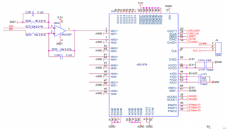
1. As shown in the following picture, I want to see if my approach will work. I am converting a differential signal into single mode signal of 1V and injecting into the ADC ADS1278. The Signal can not go negative because the OPAM OPA2387 is single side biased. I want to confirm if this approach will work ?

2. The ADC will be interfaced with TIVA TM4C129 SPI port, Can I use the Syn Pin to hold the ADC and release for start of conversion when required ? If not how can I keep the ADC on hold and then start a conversion ?  

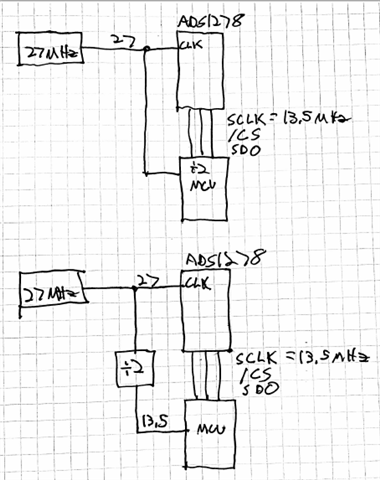
3. The SPI will be communicating at 10MHz Clock supplied by the controller to the ADC on Pin SCLK while the ADC be connected to a free running 27MHz Crystal via J9 connector. The ADC will be in High Resolution Mode. Will it work this way in High Resolution mode?

Thanks 

  • Hello,

    You can drive the input of the ADS1278 single ended.  In this mode, you should connect the AINN to a 2.5V reference bias.  In this mode, the AINP can swing from 0V to 5V, which will be interpreted as a +/-2.5V differential input.

    The ADS1278 continuously converts.  The host MCU should monitor the DRDY line and retrieve data when DRDY is asserted.  You can use the SYNC pin to hold off conversions, but then you must wait for the digital filter to settle, which will significantly slow down your output data rate.

    For best performance, the host MCU SCLK should be derived from the same clock as the 27MHz main clock, and should be 1/2, 1/4, etc. of the value for best performance.  You can use a free running 27MHz oscillator for the main clock and a 10MHz SCLK, but you will see spurs in the spectrum as a result.

    Regards,
    Keith Nicholas
    Precision ADC Applications

  • Hello,

    A few additional comments.

    You should add an RC filter between the output of the amplifier and the input of the ADC.  R=50ohm and C=1nF will be a good starting point, but the values may need adjusted for best performance.  If you keep the AINN connected to ground, then you will be limited to an input range of 0V to 2.5V.

    Also, looking at your schematic, I noticed that you have AGND and DGND separated in the schematic.  For this part, both grounds must connect to the same ground plane.  If you have separate grounds planes, then all ground connections on the ADS1278 should connect to the analog ground plane.

    Regards,
    Keith

  • Hi Keith,

    Thank you for your reply. The uController will be acting as Master SPI and the ADC will be slave SPI which means the uController will be generating the SCLK for SPI and which means the uController can not be configured to act as Master and yet receive the clock instead.

    This means, I will have to implement a network that generates 20MHz from 10MHz SCLK and feed it to the ADC CLK to avoid spurs in the spectrum. However I am not sure how can I double the clock from SCLK line to produce twice clock of SCLK to feed to CLK line. Please suggest any reference etc.

    Thanks

    Regards,

    Sahil

  • Hello Sahil,

    Use an external crystal oscillator to provide the main clock to the ADS1278 and the MCU.  The MCU can then divide this clock down to 13.5MHz for the SPI SCLK.  If 27MHz frequency is too high for the MCU clock, then you can divide it externally with a D flip flop, and supply the MCU directly with 13.5MHz.

    The ADS127L01EVM shows a similar approach with the ADS127L01 and the TM4C1294 MCU.

    Regards,
    Keith

  • The controller is running at 25MHz Main clock input which is connected to internal PLL to generate 120MHz clock for the processor.

    Taking similar approach as shown in the first approach in the picture you shared by feeding that same clock of 25MHz to the ADC and running SPI at 12.5MHz (half of Main clock) will work in High Resolution mode of the ADC and avoiding spurs in the ADC spectrum as ADC recommends to use 27MHz specifically for the High Resolution mode?

    Referring to your earlier comments on AGND and DGND, both grounds are meeting via 0R resistor.

  • Hi Sahil,

    Yes, you can use the 25MHz Main clock to also clock the ADS1278 in High resolution mode.  The only difference will be the output data rate.  In high resolution mode, you will now get:

    Fdata = Fclk/512 = 25M/512 = 48828sps.

    Operating SCLK at 12.5MHz will meet the requirement of SCLK/FCLK = 1, 1/2, 1/4, 1/8, ... to avoid spurs in ADC spectrum.

    It is best to tie both AGND and DGND pins of the ADS1278 directly to the AGND plane in the board.  If you connect through a 0R resistor directly next to the IC package, the device will function correctly, but may be more susceptible to ESD and over-voltage transients.

    Here is a previous e2e post that discusses this in more detail:

    ADS1278 Ground Connection

    Regards,
    Keith

  • Hi Keith,

    Thank very much for your help. You have a great weekend.