This thread has been locked.

If you have a related question, please click the "Ask a related question" button in the top right corner. The newly created question will be automatically linked to this question.

ADC3660: ADC3660 acquisition result is a constant value

Part Number: ADC3660

1. Use the environment

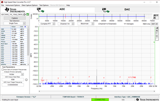
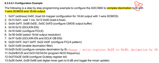
The ADC3660 is configured with 1Wire, 16bit, FS=65MHz, DCCLKIN=65MHz, 16 complex Decimation

2. problems

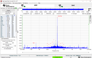
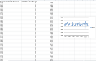
External to the ADC a sinusoidal signal, ADC acquisition result is basically unchanged, is a constant value.When the board is not powered on, use an oscilloscope to test PIN 38 39, that is, BINP BINM input signal is OK.After the board is powered on, the input signal is drowned by noise.

signal schematic

signal path PCB

  • Hi,

    Can you share a picture of the noise you are seeing? What are the registers you are writing in order to configure the ADC in 1 wire decimation mode?

    Here is an FFT of the complex data with a 10 MHz NCO applied (no analog input present).

    Here is an FFT of the complex data with a 10 MHz NCO applied, and a 10.1 MHz analog input applied.

    Using the ADC3660EVM, I have programmed the ADC registers with the following values to enable your settings (with 10 MHz NCO).

    Writing register 0x7 to 0x6c

    Writing register 0x7 to 0x6c

    Writing register 0x13 to 0x1

    Writing register 0x13 to 0x0

    Writing register 0x7 to 0x6c

    Writing register 0x1b to 0x88

    Writing register 0x1b to 0x88

    Writing register 0x19 to 0x82

    Writing register 0x19 to 0x82

    Writing register 0x19 to 0x82

    Writing register 0x1f to 0x50

    Writing register 0x1f to 0x50

    Writing register 0xa to 0x7f

    Writing register 0xb to 0xee

    Writing register 0xc to 0xfc

    Writing register 0xc to 0xfc

    Writing register 0x18 to 0x10

    Writing register 0x20 to 0xff

    Writing register 0x21 to 0xff

    Writing register 0x22 to 0xf

    Writing register 0x19 to 0x82

    Writing register 0x24 to 0x7

    Writing register 0x24 to 0x7

    Writing register 0x24 to 0x7

    Writing register 0x24 to 0x7

    Writing register 0x27 to 0x8

    Writing register 0x2e to 0x8

    Writing register 0x27 to 0x8

    Writing register 0x2e to 0x8

    Writing register 0x25 to 0x20

    Writing register 0x25 to 0x20

    Writing register 0x25 to 0x20

    Writing register 0x2a to 0x27

    Writing register 0x2b to 0x76

    Writing register 0x2c to 0x62

    Writing register 0x2d to 0x27

    Writing register 0x31 to 0x27

    Writing register 0x32 to 0x76

    Writing register 0x33 to 0x62

    Writing register 0x34 to 0x27

    Writing register 0x26 to 0xa8

    Writing register 0x26 to 0xaa

    Writing register 0x26 to 0x8a

    Writing register 0x26 to 0x88

    Register value of 0x7 is 0x0

    Writing register 0x7 to 0x0

    Writing register 0x26 to 0x88

    Writing register 0x26 to 0x88

    Writing register 0x26 to 0x88

    Writing register 0x26 to 0x88

    Writing register 0x25 to 0x40

    Writing register 0x2a to 0x27

    Writing register 0x2b to 0x76

    Writing register 0x2c to 0x62

    Writing register 0x2d to 0x27

    Writing register 0x31 to 0x27

    Writing register 0x32 to 0x76

    Writing register 0x33 to 0x62

    Writing register 0x34 to 0x27

    Please try these settings, and see if it corrects your issue.

    You can also enable the ramp test pattern to ensure that the data is being processed correctly in your FPGA. Here are the register writes.

    Writing register 0x14 to 0x4

    Writing register 0x15 to 0x0

    Writing register 0x16 to 0x48

    Best regards,

    Dan

  • thank you very much for your reply, I will review my design and feedback when i get the result

  • 1. Above is my configuaration.using the axample.

    2.Don't understand why the GUI software or the configuration you give has a lot of repeated configuration procedures, such as Writing Register 0x7 to 0x6c.

    3. below is my data process code 

    module AD_Data_Pro
    (
        input              test_clk130MHz,
        input              I_rst       ,
    	input 			   I_dclk		,
    	input 			   I_fclk		,
    	input			   I_da6		,
    	input			   I_db6		,
    	output reg [15:0]  adc_data	,
    	output 			   adc_dvld 
    );


    reg  [15:0] chb_data	 ; 
    reg  [15:0] fclk_data    ;


    always@(posedge I_dclk)begin
    	if(I_rst==1'b1)begin
    		fclk_data<='d0;
    	end 
    	else begin
    		fclk_data<={fclk_data[14:0],I_fclk};
    	end 
    end 	
    	
    always@(posedge I_dclk)begin
    	if(I_rst==1'b1)begin
    		chb_data<='d0;
    	end 
    	else begin
    		chb_data<={chb_data[14:0],I_db6};
    	end 
    end
    
    always@(posedge I_dclk)begin
        adc_data<=chb_data;
    end 
    
    reg data_vld;
    
    always@(posedge I_dclk)begin
    	if(I_rst==1'b1)begin
    		data_vld<='d0;
    	end 
    	else if (fclk_data==16'hff00)begin
    		data_vld<='d1;
    	end 
    	else begin
    		data_vld<='d0;
    	end 
    end

  • External analog source input 250KHz sine wave

  • Excel draws a waveform that is not a sine wave

    250KSPS_data_process.csv

  • Hi,

    What is the NCO frequency that is being used? Can you please use the real decimation configuration and verify that the 250 kHz signal is present in the FFT?

    Best,

    Dan