I am trying to use the same settings in the EVK FPGA firmware as in the code executed by our micro while it is driving the DDC114, in order to check that we get the same sample value & noise. However, I am struggling to relate the GUI settings back to our code. The Userguide
Our micro code sets the integration time to a time which when it times out, flips the CONV bit, & this time is in nanoSecs. The DDC then integrates & DVALID goes true when its got a result.
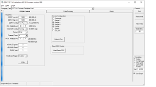
In order to exercise the DDC with the FPGA GUI, I need to set the register group, but its difficult to tell what is divided by what to get the numbers in the right place...
Is MCLK divided to form CLK, and then this is in turn divided to form CONV?
And as for the divisors,
Is the clock, MCLK, divided by the number of cycles given in CLK High + 1 + CLK Low +1, in order to produce CLK? So an MCLK of 80MHz, divided by 9 & 9 as stated in the UI is actually divided by 20, resulting in 4MHz?
The derived CLK of 4MHz gives a divider output with period of 250nSecs. Dividing by 1600 cycles of 250nS (ie 1600 Low Int & 1600 High Int) gives 400uS Low & similarly for High - is that the equivalent of an integration time of 800uS?.