This thread has been locked.

If you have a related question, please click the "Ask a related question" button in the top right corner. The newly created question will be automatically linked to this question.

ADS1261: SPI C2000

Part Number: ADS1261
Other Parts Discussed in Thread: SYSCONFIG

Hi everyone,

I am trying to get to work the ADS1261 with a C2000 (F28388D).

I started from SPI loopback example project and add the ADS1261 C library available (sbac199).

  1. My SPI config is as below:

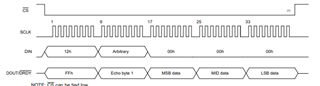
    Protocol : PROT POL0PHA1

    STE Polarity: SPISTE is active low (normal)

    Emulation Mode: EMULATION STOP AFTER TRANSMIT

    Bite Rate 1000000Hz

    Data Width: 8bit

    Use FIFO

  2. edited all of the function contents inside the interface.c  with the name of my pins.

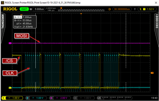
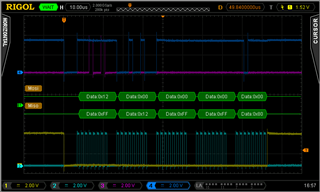
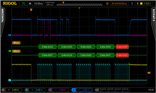
If I try to call the function ads1261_enable_internal_reference_example(); when the code goes to setCS my pin nCS does not goes low.

I edited setCS as follow:

void setCS(bool state)
{
    /* --- INSERT YOUR CODE HERE ---
     * This function sets the "nCS" GPIO pin state,
     * according to the input argument, and delays for 50 ns.
     *
     * The following code shows an example using TivaWare™...
     */

    if (state)
	{
        /* Sets the nCS pin HIGH */
        //GPIOPinWrite(SPI_STEn, nCS_PIN, nCS_PIN);
        GPIO_writePin(GPIO_PIN_SPIA_STEN,1);

	}
	else
	{
	    /* Sets the nCS pin LOW */

		GPIO_writePin(GPIO_PIN_SPIA_STEN,0);
		GPIO_writePin(GPIO3,0); //DEBUG
	}

    /* td(SCCS)/td(CSSC) delay */
    DEVICE_DELAY_US(8);
    //SysCtlDelay(2);

}

it looks like GPIO_writePin(GPIO_PIN_SPIA_STEN,0); does not work.

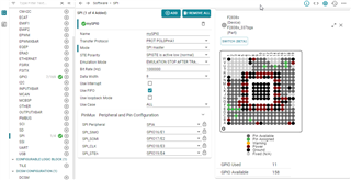
I use SysConfig to configure my pinout, in board.c I see the SPI_init and Pinmux_init:

/*
 * Copyright (c) 2020 Texas Instruments Incorporated - http://www.ti.com
 * All rights reserved.
 *
 * Redistribution and use in source and binary forms, with or without
 * modification, are permitted provided that the following conditions
 * are met:
 *
 * *  Redistributions of source code must retain the above copyright
 *    notice, this list of conditions and the following disclaimer.
 *
 * *  Redistributions in binary form must reproduce the above copyright
 *    notice, this list of conditions and the following disclaimer in the
 *    documentation and/or other materials provided with the distribution.
 *
 * *  Neither the name of Texas Instruments Incorporated nor the names of
 *    its contributors may be used to endorse or promote products derived
 *    from this software without specific prior written permission.
 *
 * THIS SOFTWARE IS PROVIDED BY THE COPYRIGHT HOLDERS AND CONTRIBUTORS "AS IS"
 * AND ANY EXPRESS OR IMPLIED WARRANTIES, INCLUDING, BUT NOT LIMITED TO,
 * THE IMPLIED WARRANTIES OF MERCHANTABILITY AND FITNESS FOR A PARTICULAR
 * PURPOSE ARE DISCLAIMED. IN NO EVENT SHALL THE COPYRIGHT OWNER OR
 * CONTRIBUTORS BE LIABLE FOR ANY DIRECT, INDIRECT, INCIDENTAL, SPECIAL,
 * EXEMPLARY, OR CONSEQUENTIAL DAMAGES (INCLUDING, BUT NOT LIMITED TO,
 * PROCUREMENT OF SUBSTITUTE GOODS OR SERVICES; LOSS OF USE, DATA, OR PROFITS;
 * OR BUSINESS INTERRUPTION) HOWEVER CAUSED AND ON ANY THEORY OF LIABILITY,
 * WHETHER IN CONTRACT, STRICT LIABILITY, OR TORT (INCLUDING NEGLIGENCE OR
 * OTHERWISE) ARISING IN ANY WAY OUT OF THE USE OF THIS SOFTWARE,
 * EVEN IF ADVISED OF THE POSSIBILITY OF SUCH DAMAGE.
 *
 */

#include "board.h"

void Board_init()
{
	EALLOW;

	PinMux_init();
	GPIO_init();
	SPI_init();

	EDIS;
}

void PinMux_init()
{
	//GPIO40 -> NDRDY Pinmux
	GPIO_setPinConfig(GPIO_40_GPIO40);
	//GPIO96 -> nRESET Pinmux
	GPIO_setPinConfig(GPIO_96_GPIO96);
	//GPIO41 -> nPWDN Pinmux
	GPIO_setPinConfig(GPIO_41_GPIO41);
	//GPIO98 -> START Pinmux
	GPIO_setPinConfig(GPIO_98_GPIO98);
	//GPIO34 -> LED_34 Pinmux
	GPIO_setPinConfig(GPIO_34_GPIO34);
	//GPIO31 -> LED_31 Pinmux
	GPIO_setPinConfig(GPIO_31_GPIO31);
	//GPIO3 -> GPIO3 Pinmux
	GPIO_setPinConfig(GPIO_3_GPIO3);
	//SPIA -> mySPI0 Pinmux
	GPIO_setPinConfig(GPIO_16_SPIA_SIMO);
	GPIO_setPinConfig(GPIO_17_SPIA_SOMI);
	GPIO_setPinConfig(GPIO_18_SPIA_CLK);
	GPIO_setPinConfig(GPIO_19_SPIA_STEN);

}

void GPIO_init(){
		
	//NDRDY initialization
	GPIO_setDirectionMode(NDRDY, GPIO_DIR_MODE_IN);
	GPIO_setPadConfig(NDRDY, GPIO_PIN_TYPE_STD);
	GPIO_setMasterCore(NDRDY, GPIO_CORE_CPU1);
	GPIO_setQualificationMode(NDRDY, GPIO_QUAL_SYNC);
		
	//nRESET initialization
	GPIO_setDirectionMode(nRESET, GPIO_DIR_MODE_OUT);
	GPIO_setPadConfig(nRESET, GPIO_PIN_TYPE_STD);
	GPIO_setMasterCore(nRESET, GPIO_CORE_CPU1);
	GPIO_setQualificationMode(nRESET, GPIO_QUAL_SYNC);
		
	//nPWDN initialization
	GPIO_setDirectionMode(nPWDN, GPIO_DIR_MODE_OUT);
	GPIO_setPadConfig(nPWDN, GPIO_PIN_TYPE_STD);
	GPIO_setMasterCore(nPWDN, GPIO_CORE_CPU1);
	GPIO_setQualificationMode(nPWDN, GPIO_QUAL_SYNC);
		
	//START initialization
	GPIO_setDirectionMode(START, GPIO_DIR_MODE_OUT);
	GPIO_setPadConfig(START, GPIO_PIN_TYPE_STD);
	GPIO_setMasterCore(START, GPIO_CORE_CPU1);
	GPIO_setQualificationMode(START, GPIO_QUAL_SYNC);
		
	//LED_34 initialization
	GPIO_setDirectionMode(LED_34, GPIO_DIR_MODE_OUT);
	GPIO_setPadConfig(LED_34, GPIO_PIN_TYPE_STD);
	GPIO_setMasterCore(LED_34, GPIO_CORE_CPU1);
	GPIO_setQualificationMode(LED_34, GPIO_QUAL_SYNC);
		
	//LED_31 initialization
	GPIO_setDirectionMode(LED_31, GPIO_DIR_MODE_OUT);
	GPIO_setPadConfig(LED_31, GPIO_PIN_TYPE_STD);
	GPIO_setMasterCore(LED_31, GPIO_CORE_CPU1);
	GPIO_setQualificationMode(LED_31, GPIO_QUAL_SYNC);
		
	//GPIO3 initialization
	GPIO_setDirectionMode(GPIO3, GPIO_DIR_MODE_OUT);
	GPIO_setPadConfig(GPIO3, GPIO_PIN_TYPE_STD);
	GPIO_setMasterCore(GPIO3, GPIO_CORE_CPU1);
	GPIO_setQualificationMode(GPIO3, GPIO_QUAL_SYNC);
}
void SPI_init()
{
	
	//mySPI0 initialization
	SPI_disableModule(mySPI0_BASE);
	SPI_setConfig(mySPI0_BASE, DEVICE_LSPCLK_FREQ, SPI_PROT_POL0PHA1,
				  SPI_MODE_MASTER, 1000000, 	8);
	SPI_enableFIFO(mySPI0_BASE);
	SPI_setFIFOInterruptLevel(mySPI0_BASE, SPI_FIFO_TXEMPTY, SPI_FIFO_RXEMPTY);
	SPI_disableLoopback(mySPI0_BASE);
	SPI_setEmulationMode(mySPI0_BASE, SPI_EMULATION_STOP_AFTER_TRANSMIT);
	SPI_enableModule(mySPI0_BASE);
}

In my main  Boars_init(); is called to do:
PinMux_init();
GPIO_init();
SPI_init();

So I am not sure what is wrong, do I need to do something else than just SPI_init()? Can you confirm GPIO_PIN_SPIA_STEN is a regular GPIO even if its defined for SPI in sysConfig?

To be sure it was not hardware I started a new project and define my pin19 as a normal GPIO and it works OK I can toggle the pin.

I put my project if it can help.

Thank you

spi_ADS1261.zip

  • Hi Hal,

    Does your code configure the correct pin on the C2000 to act as the CS line?

    Are you able to probe this line and see if anything is actually toggling?

    You might also try posting this same question in the MCU forum, since it sounds like the issue is related to the MCU configuration, not the ADC (since you are able to get a GPIO to work, just not the desired control line, and since CS is a signal driven by the MCU).

    -Bryan

  • Hy Bryan,thanks for helping.

    I actually found that my SPI pins were not initialized by the code generated by SysConfig, which is weird.

    So I added for CS, SIMO, SOMI and CLK with the right init and it looks OK now on the oscillo I can see the CS going low.

    I have some others questions;

    • Do you recommend the use of FIFO and SPI routine interrupts? The other option would be to wait in a loop waiting on RX data?
    • As I showed previously, I tied START, PWDN and RESET pin to VDD, so it means it runs directly in continuous mode.
      I try to avoid to configure any registers in the first time to make it easier. Could you confirm that with the default register values it should be enough to just monitor the DRDY and read data when DRDY goes low?

    Thank you
     

  • Hi Hal,

    Glad you resolved the initial issue

    I am not sure that I would recommend one over the other, it would really depend on what your overall application needs to accomplish e.g. if you have other routines running then an interrupt-driven approach might make more sense. If you just want to read out data from the ADC, it probably doesn't matter either way (on several occasions I have seen other people using loops waiting for DRDY to drop low).

    If you leave all of the registers at their default settings, everything would be okay except for the input mux (see figure below). The mux channels default to a short to VCOM, so you would be reading 0 V (this is really how you would measure the noise of the ADC). In other words, you would not be able to read an input signal with the default settings. You could use the default settings to confirm the noise performance from the ADC datasheet, at a gain of 1, 20 SPS, and FIR filter (should be ~370nVRMS).

    -Bryan

  • Thank you so much Bryan for your help.

    I noticed in ADS1261.c the readData function has array argument  but the description are pointers:

    In my main I initialized three arrays:

        uint8_t status[1];
        uint8_t data[20];
        uint8_t crc[10];

    and call the function in my loop:

    while(1){
            result = readData(status,data,crc);
            for (cpt=4;cpt>0;cpt--)
            {
                //GPIO_writePin(LED_34, cpt & 0x1);
                DEVICE_DELAY_US(cpt*100000);
            }

    If I probes MISO CLK and /CS I would expect to see:

    But the MOSI does not go high:

    I check the hardware by replacing the MOSI pin by a regular GPIO and I am able to toggle the pin.

    My guess is I did something wrong when I re-write the function SPI_SendReceive(DataTx, DataRx, byteLength); in interface.c:

    void SPI_SendReceive(uint8_t *DataTx, uint8_t *DataRx, uint8_t byteLength)
    {
       /*	--- INSERT YOUR CODE HERE ---
    	*
    	* 	This function should send and receive multiple bytes over the SPI.
    	*
    	* 	A typical SPI send/receive sequence may look like the following:
    	* 	1) Make sure SPI receive buffer is empty
    	* 	2) Set the /CS pin low (if controlled by GPIO)
    	* 	3) Send command bytes to SPI transmit buffer
    	* 	4) Wait for SPI receive interrupt
    	* 	5) Retrieve data from SPI receive buffer
    	* 	6) Set the /CS pin high (if controlled by GPIO)
    	*
    	*/
    
    	/* Set the nCS pin LOW */
    	setCS(LOW);
    
    	/* Remove any residual or old data from the receive FIFO */
    	uint32_t junk;
    	//while (SSIDataGetNonBlocking(SSI0_BASE, &junk));      /*COMMENTED*/
    	//while (SPI_readDataBlockingNonFIFO(SPIA_BASE, &junk));/*COMMENTED*/
    
    
    	int i;
    	for (i = 0; i < byteLength; i++)
    	{
    		/* Set up data for the next transmit */
    		//HWREG(SSI0_BASE + SSI_O_DR) = DataTx[i];          /*COMMENTED*/
    		SPI_writeDataBlockingNonFIFO(SPIA_BASE, DataTx[i]); /*REPLACED BY*/
    		
    		/* Wait for data to appear */
    		//while (!(HWREG(SSI0_BASE + SSI_O_SR) & SSI_SR_RNE)); /*COMMENTED*/
    
    		/* Grab the return data */
    		//DataRx[i] = HWREG(SSI0_BASE + SSI_O_DR);          /*COMMENTED*/
    		DataRx[i] = SPI_readDataBlockingNonFIFO(SPIA_BASE); /*REPLACED BY*/
    	}
    
    	/* Set the nCS pin HIGH */
    	setCS(HIGH);
    }

    I basically add 

    SPI_writeDataBlockingNonFIFO(SPIA_BASE, DataTx[i]);
    
    DataRx[i] = SPI_readDataBlockingNonFIFO(SPIA_BASE);

    Also the waveform shows 5 different packets that correspond to the byteLength with no CRC so this looks good. My concern is the /CS pin, it's supposed to stay low during the whole sending, if the SPI_SendReceive function CS goes low send all the data and then CS go high...

    I am slowly getting there Grinning

  • Hi Hal,

    Glad to know you are making progress.

    You certainly do not want to toggle CS during the data read transaction. This resets the serial interface (see section 9.5.1.1 in the datasheet). It is not clear to me where the CS is being toggled in the code, so hopefully you are able to track down this line of code and rewrite it.

    -Bryan

  • Hi Bryan thanks for all your help.

    I finally got it to work and read stuff:

    For the /CS I used a regular GPIO, I don't know why but by using the GPIO_19_SPIA_STEN defined with the SPI it toggles /CS after one byte so as you said it reset the serial interface. I will check that later...

    I also had to change the SPI config to: SPI_PROT_POL0PHA0 even if it is specified in the ADS1261 that it use  SPI_PROT_POL0PHA1


        // SPI configuration. Use a 2MHz SPICLK and 8-bit word size.
        //
        SPI_setConfig(SPIA_BASE, DEVICE_LSPCLK_FREQ, SPI_PROT_POL0PHA0,
                      SPI_MODE_MASTER, 500000, 8);
    

    If I use SPI_PROT_POL0PHA1 the data are wrong (0x24 instead of 0x12) but you see that the slave is actually doing the Echo Byte 1:

    Anyway, I am going to continue playing with registers, it should be ok now.

    Thanks for the support.

  • Hi Hal,

    Yes I have seen in the past that some MCUs use different nomenclature to mean different things. For example, some MCUs might require you set CPOL = 0 and CPHA = 0 in order to be what we consider SPI mode 01. Ultimately, you just need to make sure that MCU is set such that SCLK idles low and data is read on the falling edge of SCLK, regardless of the whether this is considered mode 00, mode 01, etc.

    But it sounds like you have gotten this resolved and are making progress. Please let us know if you need anything else. If you have another issue that is unrelated to this specific thread, please feel free to start a new thread and we will assist you there.

    -Bryan