This thread has been locked.

If you have a related question, please click the "Ask a related question" button in the top right corner. The newly created question will be automatically linked to this question.

ADS112C04: SDA signal keeps Low.

Guru 11155 points
Part Number: ADS112C04
Other Parts Discussed in Thread: ISO1640, ADS1119, ADS122C04EVM

Hi team,

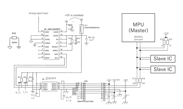
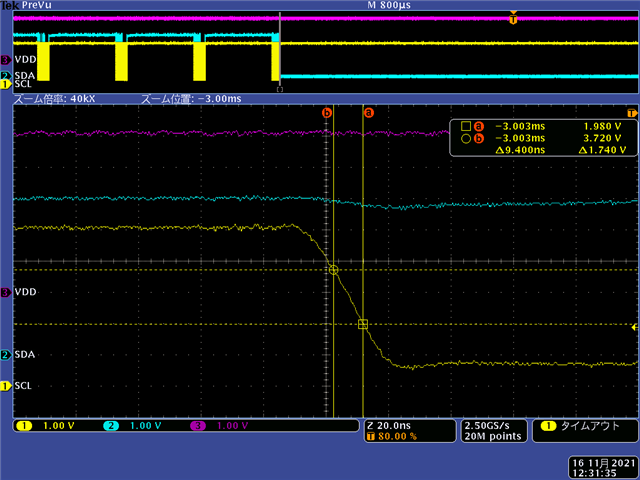
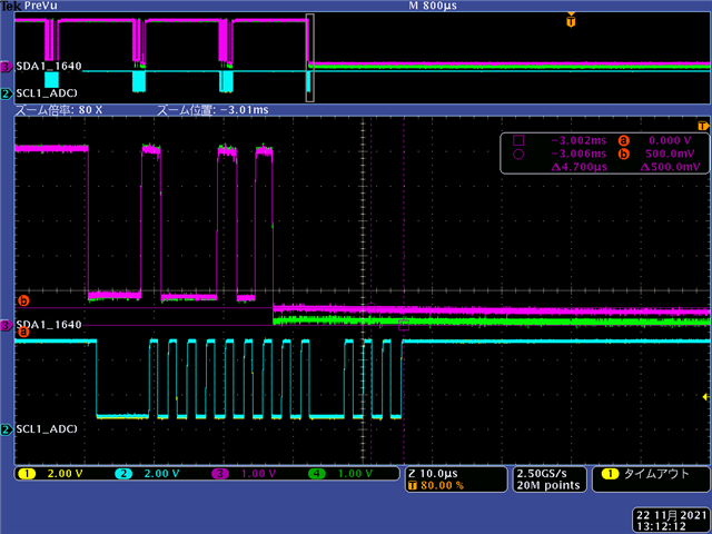
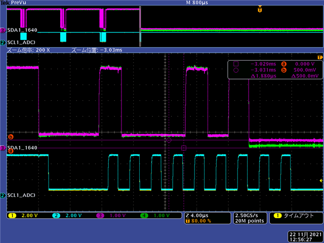
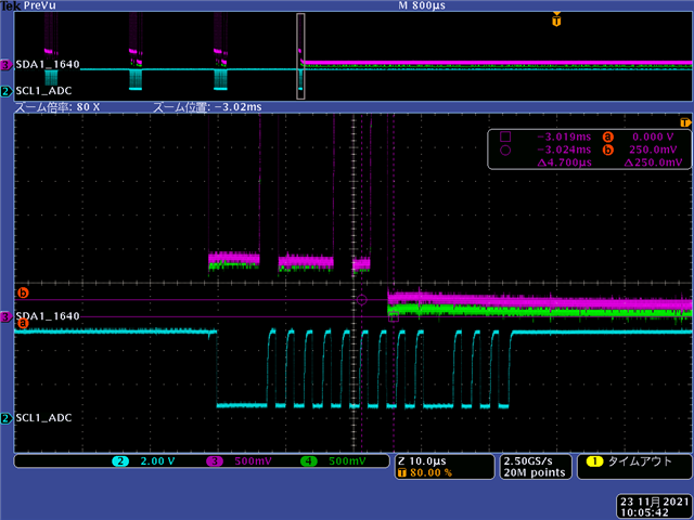
ADS112C04 keeps the SDA signal Low.
Why does this happen?

Purple: DVDD
Yellow :SCL
Blue :SDA


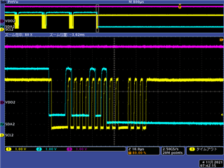
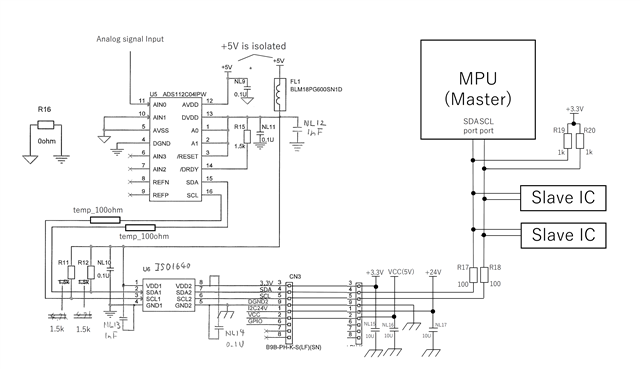
There is ISO1640 between MCU and ADS112C04 and GND of MCU side is rising.

Sincerely.
Kengo.

  • Hi Kengo,

    It is difficult to say what might be happening here.  Can you send me the schematic?  What side of the isolator (MCU or ADS112C04) were the scope probes applied?  Is the reset pin on the ADS112C04 pulled high?

    As far as SDA going low, according to the scope plot this is happening during the addressing but before the address has been completed and the device would normally ACK.  Are there any other devices on the I2C bus that could interfere?

    Best regards,

    Bob B

  • Hi Bob,

    Thank you so much for your usual support.
    I'll check with my customer.
    If I get the schematic, I'll share it with you in a private message.

    Sincerely.
    Kengo.

  • Hello Mr. Benjamin,

    I'm Kengo customer's engineer.

    Kengo gives me permission to send direct message to you.

    So, I reply your question and share schematic directly.

    Q1. Can you send me schematic ?

    A1. I attached below. Very happy if you found any concerns or have comments and let me know. That would help me.

    Q2. What side of the isolator (MCU or ADS112C04) were the scope probes applied?

    A2. I probed scope on side1 of ISO1640(i.e. ADS112C04) and recorded that waveform.

    Q3. Is the reset pin on the ADS112C04 pulled high?

    A3. Pulled high (See schematic.)

    Q4. Are there any other devices on the I2C bus that could interfere?

    A4. I allocated different slave addresses for three devices. 

    Then, I think there is no possibility any other devices on the same I2C bus interfere.

    I found similar phenomenon in E2E of ADS1119.

    https://e2e.ti.com/support/data-converters-group/data-converters/f/data-converters-forum/985791/ads1119-i2c-communication-error?tisearch=e2e-sitesearch&keymatch=ads1119#

    At above link, it seems like the user of ADS1119 uses isolator that can be assumed from waveform.

    However, it seems like you and user couldn't reach conclusion at that time.

    Then, I'm afraid something happens when we insert isolation IC between MCU and TI's ADC IC.

    I would like to discuss this phenomenon further with you on this E2E and reach conclusion why this phenomenon happens.

    Best, 

    T. Sakakima

  • Hi Sakakima,

    Thank you for the additional information.  First I would like to say that the E2E post that you referred to with the SDA low was clearly caused by a missing 9th SCL clock from the micro which means the SDA would hold low for ACK and not release until the 9th SCL clock was received.  This is much different from the issue you are seeing.

    Your scope plots are showing that the SDA is going low one clock earlier than expected.  As there appears to be an ACK for the selected address by pulling the SDA low, there could be a glitch on the SCL line.  However, a glitch is not showing up in the scope plot.  Also, the SDA should release on the next SCL.  So there is a unique situation that may cause the ADS112C04 to be holding the SDA low.  From what has been seen in similar situations is a transient event causing an issue with the ADS112C04.

    The transient can be:

    • Picked up in wiring in a prototype configuration.  For example, if a breadboard prototype is used with loops of wire connecting the various pin connections, EMI/RFI can be picked up in the wiring.
    • Using a PCB with an insufficient ground.  The ground on the PCB is best as a solid single ground plane as opposed to a bunch of ground traces.
    • Power supply transients.  In your schematic you should a ferrite is used on the digital supply.  We have seen some issues when using ferrites in the supply as CMOS devices may use very short duration, but large current draws into the 10's of mA during various internal startup and switching configurations.  The ferrite may choke the needed current and cause a voltage droop that may cause strange operation or even reset the device.
    • A transient on the analog inputs that may exceed the absolute maximum input ratings.  ESD and EMI/RFI are common transients sources that may create an operational issue with the ADS112C04.

    It can be a difficult task in determining the exact mechanism that may be causing the issue.  It is helpful to look at each possibility and try to determine if this is the cause.  For example, eliminate the analog input by making sure that the input is not exceeding the maximum input ratings by either allowing the input to float or tie to ground.  If you no longer see erratic communication then most likely this is the cause.  If you still have the issue replace the ferrite with a 0 ohm resistor and see if that fixes the issue.  Keep trying various options to either find the source or eliminate a potential issue.

    Best regards,

    Bob B

  • Hi Bob, 

    Thank you for kind reply.

    I tried measures what you advised to fix this issue, but unfortunately I did not were succeeded in any measures.

    I don't use a breadboard. I use a PCB circuit board that have solid ground layer. All analog input has floated while I have tried to fix this issue then there was no analog signal input to ADS112C04.

    I also tried replace ferrite with 0 ohm resistor today but this issue occured...   

    As you mentioned, I also thought there was glitch in SCL from first clock to 7th clock when I faced this issue at first. Then, at 7th clock, ADS112C04 judged as if micro send 9th clock and returned ACK.

    But I didn't observe no glitch even when I expanded waveform view in scope.

    By the way, I use 500MHz bandwidth scope. So, high frequency noise over 100MHz may not able to observe correctly. 

    And you mentioned "EMI/RFI can be picked up in the wiring",  then I have one question.

    Q1. Is SCL and SDA of ADS112C04 affected by high frequency noise or harmonized waveform over 100MHz ?

           If so, I need to reconfigure measurement environment to find whether there was over 100MHz noise or not. 

    And I need to share two information with you.

    1. When micro started communication with ADS112C04 via ISO1640, communication started correctly, and communication continue about several minutes to 30minutes, then suddenly communication fail occurs and this issue was monitored. (sometimes fail occurs in several times, sometimes communication continue about 30minutes and fail occurs suddenly. )  

    2. When I pulled out ISO1640 and connected side1 and side2 directly and isolated +5V changed to +3.3V,

        I hadn't observed this hang-up issue over 168hours(7days) since micro started communication with ADS112C04.

    From above two facts, I thought combination of ISO1640 and ADS112C04's I2C digital interface may cause this issue.

    However, I didn't catch the fact at this time. 

    If you have any more advice and comment, let me know. I'll try and check what you advise again.

    T. Sakakima

  • Hi Sakakima,

    It appears that you have reduced the variable to just the isolator.  After reviewing the datasheet for the ISO6140 I see that there is a considerable difference between side 1 and side 2.  The ISO device is optimized for side 1 to be directly connected to the micro and side 2 to the bus.  This connection makes sense if all I2C target devices were on the isolated side.  However that is not the case for your design and I would most likely connect the ISO the same way as you are showing in the schematic.

    So the drive strength on side 2 is much stronger and can overcome a larger capacitance than side 1.  If there are timing issues or drive strength issues between side 1 and side 2, there may be some tuning of components required.  For example, you have 1k pullups on the high strength drive and 4.7k pullups on the already low drive strength side.  I would connect the scope to both sides of the isolator and attempt to match any signal timing differences.  Most likely you will see slower rise and fall times on side 1 compared to side 2.  Using smaller values of resistors on side 1 may improve any differences.

    Also consider that the ISO device is both a level shifter as well as bi-directional isolator and the transition levels as to what is considered a logic high and logic low will differ from side to side.  Another thing to consider is the ISO device is not fully I2C compliant on side 1.  Side 1 is not capable of driving capacitance of more than 80pF.  If the bus capacitance becomes too large (larger than 40pF as per ISO test circuit) there could be some timing related issues.  Again, lowering the resistance may be of some help as well as lowering the SCL frequency.  It would appear from the scope plot that you are running at 400kHz SCL.  I would try lowering the frequency to 100kHz to see if there is improvement.

    Best regards,

    Bob B

  • Hi Bob,

    I appreciate you reviewed ISO1640 datasheet.

    I'll ask why ISO1640 datasheet shows micro is located in side1 of ISO1640 to TI expert in isolation forum.

    Even 4.7kohm pullup in side1 of ISO1640 and 1kohm pullup in side2 of ISO1640, there is no deviation from I2C specification.

    Of course, there is propagation delay in rising time and falling time due to ISO1640 and bus capacitance but I think that may not be cause of this issue.

    And there is no significant difference between communication success timing and fail timing as long as I reviewed waveform. (See PPTX attachment.)

    E2E_20111117_A.pptx

    I tried 4.7kohm pullup at 100kHz and 1.5kohm pull up in side1 at 400kHz and 100kHz, however, communication failed suddenly and same waveform was monitored in every condition. 

    But I found one thing in falling time of ISO1640. That is falling time of side1 seems to be too fast.

    According to I2C specification and datasheet of ADS112C04, fall time of both SDA and SCL signal should be over 20ns * (VDD / 5.5V).

    In this case, VDD of SCL consider 4.3V because diode in ISO1640 float 0.7V.

    Then, fall time should be over 20ns * 4.3V / 5.5V = 15.6ns. 

    However, When I measured SCL falling time, that is about 10ns. See image attachment. *1)

    *1) In this case we consider 0.7VDD = 0.7 * (5.0 - 0.7)V + 0.7V = 3.71V, also 0.3VDD = 0.3V * (5.0 - 0.7)V * 0.7V = 1.99V.

    As far as I investigated from websites, the purpose of the specification is to help mitigate EMI. 

    So, I suppose that is not a must to follow. 

    However, I am a little concerned whether this short falling time affect ADS112C04's operation.

    And this is my question for you at this time.

    Other questions on ISO1640, I'll ask in TI expert in isolation forum.

    If you have any other advices and comments, let me know again.

    Thank you very much for your corporation.

    Best,

    Toshihiro  

  • Hi Toshihiro,

    Thanks for the data and scope shots.  There is definitely a strange behavior happening on SDA.  Just so I'm clear on what is happening, are you saying that when operating at 100kHz SCL the failure rate is worse than you were seeing at 400kHz?

    It does appear that the SDA is going low on side 1 before going low on side 2 which would indicate that the ADS112C04 is driving it low.  However if this is the case then I don't understand why SDA doesn't release on the next clock cycle.  It would be good to somehow verify that the ADS112C04 is truly holding the SDA low.  This may be difficult to do on your board, but if you could add a jumper between the isolator and the ADS112C04 you could remove the jumper at the time of failure to see if the ADS112C04 SDA line goes back high.

    Another experiment that could be done is to put a pullup on the RESET pin instead of a direct connection to DVDD so that the pin could be shorted temporarily to reset the device.  A reset on the ADS112C04 should also for a reset on the SDA pin.

    These actions will help to verify that the issue is related to the ADS112C04 and not a latch condition on the output of the ISO1640.  The ISO1640 datasheet says the bypass caps to the VCC supply pins should be 2mm or less.  Are your bypass caps within this spacing?  And do the caps connect directly at the ISO pins or are they on the opposite side of the board with a via in between?

    I'll keep thinking of what might be happening, but I'm quickly running out of ideas and things to try.  As far as I can tell there should not be a problem with this configuration.

    Best regards,

    Bob B

  • Hi Bob,

    Thank you for your lots of comments and advises.

    I think they might be very difficult tasks what you advise using our board ; 

    1. Add a jumper between the isolator and the ADS112C04 you could remove the jumper at the time of failure to see if the ADS112C04 SDA line goes back high

    2. Another experiment that could be done is to put a pullup on the RESET pin instead of a direct connection to DVDD so that the pin could be shorted temporarily to reset the device.

    And I need to take statistics to compare 100kHz results and 400kHz results to say failure rate.

    Then I also need to take some time how to proceed to solve this issue from now and set priority because resource of samples and man-hours are limited.

    I'll discuss your advises and what I've done in this week in my team meeting on tomorrow or next Monday.

    Then I'll try what you advised and take failure rate.

    So, I'll be back discussion with you on this E2E in next week and show experiment and measurement results.

    Again, Thank you very much for your corporation.

    Best regards,

    Toshihiro

  • Hi Toshihiro,

    A colleague suggested that for item 1, instead of a jumper use a resistor (about 100 Ohms) to use as a measurement point between the isolator and the ADS112C04 and then measure the voltage difference on each side of the resistor.  This suggestion will be a lot easier to conduct as an experiment and will give us the information we need as to which device is pulling low by following the direction of current flow.

    Best regards,

    Bob B

  • Hi Bob, 

    Thank you for your proposal.

    I somehow inserted 100ohms resistor like the figure below("temp_100ohm" means inserted 100ohm).

    (And R11 and R12 were replaced by 1.5kohm resistors, and FL1 was replaced by 0ohm resistor.)

    Here is the result.

    Purple line : ISO1640 side of temp_100ohm in SDA line

    Green line : ADS112C04 side of temp_100ohm in SDA line

    Blue line : ADS112C04 side of temp_100ohm in SCL line

    And here is expanding picture from start condition to 9th clock of SCL,

    The purple line was floated to 0.5V from GND level after 7th clock of SCL.

    I will try to interpret this result tomorrow.

    If you have any questions or comments, let me know.

    Best regards,

    Toshihiro  

  • HI Toshihiro,

    Thanks for the additional information and screen shots.  I will have to see if I can duplicate this same behavior using the same kind of configuration as you are using.  However this will take same time for me to do so as I will need to procure the ISO1640 and connect it to my experimental hardware.  Also this week is a holiday week in the USA.  It will probably take me a couple of weeks to get this hardware set up and tested.  Any additional information you can gather would be helpful.

    Best regards,

    Bob B

  • Hi Bob,

    Thank you for your continuous support.

    First, I appreciate your effort for trying and confirming whether this issue occur or not in your environment.

    --------------------------------------------------------------------------------------------------

    I tried to clarify which side device pulling low more clearly today. 

    I replaced 1.5kohm R11 and R12 pull up resistor with 4.7kohm.

    Then here is the result in below attachment (expanding voltage division of SDA line snapshot).

    Purple line : ISO1640 side of temp_100ohm in SDA line(500mV/div)

    Green line : ADS112C04 side of temp_100ohm in SDA line(500mV/div)

    Blue line : ADS112C04 side of temp_100ohm in SCL line(2V/div)

    The result is reasonable to explain ADS112C04 pulls low because : 

    When ADC112C04 SDA port open drain pulls, DVDD voltage is divided : 5V(DVDD) / (4.7k + 0.1k) * 0.1k = 0.1V

    and according to ADS112C04 datasheet, VOL floated 0.15V( typ, IOL = 3mA ).

    also it seems like green line floated to 0.15V in above snapshot.

    Then voltage at ISO1640 side of temp_100ohm will be 0.1V + 0.15V = 0.25V.

    If ISO1640 pulls low, the voltage of SDA line should be over 570mV (VOL in datasheet) due to a internal diode.

    So, I think ADS112C04 pulls low continuously after 7th clock of SCL.

    ----------------------------------------------------------------------------------------------------

    So far, Those results I have mentioned is I have already tried to clarify this issue.

    I understand you need to take couple of weeks to set up and test.

    If I find other information and results while you set up experiment, I'll share with you in this E2E. 

    Thank you very much in advance. 

    Best regards,

    Toshihiro

  • Hi Toshihiro,

    I received the ISO EVM and connected it to the ADS122C04EVM.  This is the 24-bit version of the ADS112C04.  So far after many hours of testing I have not seen any issues.  So I am not able to duplicate the issue you are seeing.

    I will continue to conduct tests, but so far I have not had any issues with SDA stuck low.

    Best  regards,

    Bob B

  • Hi Bob,

    Thank you for your continuous support.

    I'll take New Year's holiday and be back to my office from Jan/6/2022.

    If you have any reply or new test results, please update this E2E thread.

    I'll read your comment at this thread at Jan/6.

    Best regards,

    Toshihiro Sakakima

  • Hi Bob,

    Now I'm back to our office from Jan/6.

    I suppose you continue tests with ADS122C04EVM after U.S. holiday vacation.

    I appreciate if you could share progress or results of your tests.

    Best regards,

    Toshihiro Sakakima

  • Hi Toshihiro,

    Yes I have been testing all week and analyzing data.  What I think is happening is due to timing or threshold levels, or perhaps a combination of both.  I think there is something happening as it relates to logic levels with respect to voltage level translation.

    I have collected many hours (actually days) of data where both VDD1 and VDD2 are operating at 3.3V voltage levels and see no issues.  When I switch the ADS1x2C04 to 5V, there are random issues.  Sometimes it is SDA and sometimes it is SCLK.  

    I have seen issues with level translation before with I2C and I think something similar is happening here.  Theoretically this should work, but with signals being bi-directional, timing and logic levels can cause issues.  Sometimes this can be corrected using various combinations of pullups and bus capacitance, but once an issue is seen there can be risk as it is difficult to determine what happens with respect to the controller and how the target devices will respond.

    I will continue to investigate this, but as having the same supply voltage value on both sides of the isolator appear to have excellent response I would recommend that you use 3.3V for the digital and 5V only for the analog for the ADS112C04.

    Best regards,

    Bob B

  • Hi Bob,

    Sorry for delay reply.

    Thank you for sharing your experiment result and recommendation use for our application of ADS112C04.

    My colleague carry out an experiment using 3.3V for the digital and 5V for analog for ADS112C04 now.

    So far, we haven't  observed hang-up of I2c (for about 6hour).

    However, I think this circuit configure is temporally countermeasure for this issue. 

    Now I have questions.

    Q1. If TI find root cause of this issue, will TI redesign I2c digital IP of ADS112C04 ? 

    Q2. If TI decide to redesign digital IP, how long time will it take. Does TI have outlook now currently ?  

           (I guess if TI redesign chip, it will take amount of time due to current chip shortage.)

    Best regards, 

    Toshihiro Sakakima 

  • Hi Toshihiro,

    I still believe the issue is related to the interface connection to the isolator and not to the ADS112C04 and is then an applications issue.  The ADS112C04 is fully characterized and validated to operate across the operating temperature range and supply voltage range as specified in the datasheet.  Unfortunately there is no way for all isolation and level-shifting devices to be validated along with the ADS112C04.

    As I believe this to be an applications issue I will continue to investigate as I have time.  The problem with the investigation is that there are so many variables.  Also I do not have a good working knowledge of the isolator and there are many possible combinations to investigate here as well.

    At this point believe I found a solution that works with no other system or component changes other than the supply voltage.  We also know that the combination of the isolator and the level shifting creates the issue.  This means that the issue could be created by the isolator with respect to the level shifting, timing, drive current, etc..  So even though there appears to an issue with the ADS112C04 it could be an issue with the isolator or in the way the devices are connected together.  So there is a lot of work needed to determine a root cause.

    As far as the digital IP, I2C has been used by TI for a long time.  It is not likely there is an issue with the interface nor has any other customer that I am aware of had an issue with the communication related to the ADS112C04 itself.  Even if there was an issue uncovered most likely there would be no chip revision, but instead an example use case of how to use the device with an isolator or level shifter.  

    Best regards,

    Bob B