This thread has been locked.

If you have a related question, please click the "Ask a related question" button in the top right corner. The newly created question will be automatically linked to this question.

ADC12DJ3200EVM: ADC12DJ3200 internal ramp pattern not received at FPGA side.

Part Number: ADC12DJ3200EVM
Other Parts Discussed in Thread: LMK04828

Hi team

I am using internal ramp pattern to check whether it is properly been received at the FPGA side. I am using JMODE 2, with Fs=1250 MSPS. The Serdes is operated at 5Gbps.

As per the data sheet, "In the ramp test mode, the JESD204B link layer operates normally, but the transport layer is disabled and the
input from the formatter is ignored. After the ILA sequence, each lane transmits an identical octet stream that
increments from 0x00 to 0xFF and repeats". But i see the below patterns at my end which dont look like identical with incrementing patterms.
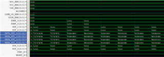
While programming the ADC card, SYNC status=1, JESD LINK=1 while reading register at address 208. Also VALID signal related to transceivers lanes (at FPGA side) is 1 which indicates that recovered data is valid.

Any idea what is happening here?

Regards

Rohit

  • Hi Rohit,

    Looking at the screen shot can check if there is buffer over flow on some of lanes? This behavior looks like your buffer is overflowing on some of the lanes. Can you make sure all the clock to the used on FPGA are coming from the same root source? 

    Regards,

    Neeraj 

  • Hi Neeraj

    Clock to the FPGA device is given from the LMK04828 oscillator on the ADC EVM board through the FMC pins. The mapping seems to be correct as I check it. I think clock is properly received on the FPGA side as the PLLs are properly locked and CDR lock is achieved for the Transceivers but there are bit errors in the data. This clearly means I am getting junk data after the ILA sequence in the screenshot I shared. Any advice on this?

    Currently i am using new ADC card REV A and using compatible ADC GUI for that. I also have REV E3 ADC card with me and plan to test using it but i am looking to find a compatible ADC GUI which i cant find online. Can you please share me compatible ADC GUI for REV E3 ADC card.

    Regards

    Rohit

  • Hi Rohit, 

    Let me see if, I can locate the revE3 version of the ADC gui and send it to you. 

    Regards,

    Neeraj 

  • Hi Neeraj

    Thanks, waiting for the rev E3 version of adc gui.

    Regards

    Rohit

  • Hi Neeraj

    I could find the old version of ADC GUI at my end and I tried with this but the behavior is same as before. I cant receive proper data at the FPGA side as there are bit errors in the data as i mentioned before. Any idea or debug step you can suggest me? I receive the CGS, ILA sequence and the SYNC signal behaves fine, but the user data is not proper.

    Regards

    Rohit

  • Hi Rohit,

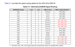
    Can you make sure the your lane mapping from ADC to FPGA is correct? Please note lane jesd lanes the polarity has been swapped for easy routing. see the table below. 

    Regards,

    Neeraj