Other Parts Discussed in Thread: TMS320F28335, ADS8568
I am confused by the SPI clock polarity and phase on ADS8528.
In the datasheet (SBAS543C pp. 33) it says:
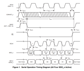
Starting with the most significant bit (MSB), the output data are changed with the SCLK falling edge.
Serial data input SDI are latched with the SCLK falling edge.
So from the MCU perspective:
- the MCU outputs data on rising edge since ADS8528 latches data on falling edge
- the MCU latches data on rising edge since ADS8528 outputs data on falling edge
Here are the supported clocking schemes for TMS320F28335 (SPRUI07 pp. 558):
Falling edge without delay. The SPI transmits data on the falling edge and receives data on the rising edge of the SPICLK.
Falling edge with delay. The SPI transmits data one half-cycle ahead of the falling edge and receives data on the falling edge of the SPICLK.
Rising edge without delay. The SPI transmits data on the rising edge and receives data on the falling edge of the SPICLK.
Rising edge with delay. The SPI transmits data one half-cycle ahead of the rising edge and receives data on the rising edge of the SPICLK.
Does this mean I have to change the clocking scheme on the master (MCU) after I write configuration? More specifically:
- to write configuration to ADS8528, I would use Falling edge with delay
- to read configuration and data from ADS8528, I would use Falling edge without delay
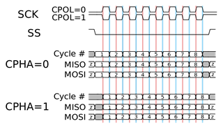
It is not mentioned in the datasheet, but from the diagrams I assume that the serial clock should idle at high. That is why I only mention the "falling edge" clocking schemes. Please correct me if I am wrong.
This is the first time I need to change clocking scheme for read and write operations. Can you please confirm this conclusion?
If I am correct about this, what would be the reason for this clocking scheme implementation on ADS8528? Why not using single clocking scheme for both read and write operations?
Let me give some perspective how I realized this in the first place.
I first configured the clocking scheme to work for "write configuration". I was reading back the configuration using the same clock scheme and it worked until I did some minor non-SPI-related change in the code.
What I mean when I say it did not work is that configuration I was reading back was not as expected. It seems the entire configuration was bit shifted to the left by 2. Again, this problem appeared only when I did some minor non-SPI-related change in the code.
Then I read the datasheet for ADS8528 again and figured the clocking scheme is different for read and write operations. I implemented this new logic and it seems to work, but I would still like to get confirmation.