This thread has been locked.

If you have a related question, please click the "Ask a related question" button in the top right corner. The newly created question will be automatically linked to this question.

ADC3664EVM: about clock input by FMC

Guru 11170 points
Part Number: ADC3664EVM

Hello E2E,

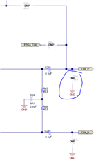
What is the assumption that the voltage of the sampling clock signal (FPGA_CLK signal input from the H4 pin of the FMC connector) input via the FMC connector is designed?

If you input a 2.5V single-ended clock with reference to VADJ-2.5V in the circuit diagram, it will exceed the rated voltage (2.1V) of the AD converter.

Since the level shifter is placed, it seems that the SPI signal etc. can input 2.5V, but the sampling clock seems to be directly connected to the AD converter. Is it okay to think that inputting as a 1.8V single-ended signal is the correct usage?

Regards,
ACGUY

  • Hi ACGUY,

    Yes, that is a correct observation. For a single-ended clock input, the voltage must not exceed 2.1Vpp (abs max), but nominally should not exceed 1.8Vpp (both with ~ +0.9V DC bias).

    Depending on the FPGA, you may be able to change the bank voltage for the FPGA clock to 1.8V, and that could satisfy this requirement.

    Otherwise, you may be able to install the termination resistor R44 to decrease the voltage swing.

    One other comment is that an FPGA clock can have nano seconds of rms jitter. This can degrade the SNR performance of the ADC, so filtering of the clock may be required to achieve desired results.

    Best Regards,

    Dan