This thread has been locked.

If you have a related question, please click the "Ask a related question" button in the top right corner. The newly created question will be automatically linked to this question.

ADS7028: Control ADS7028 via TMS320C2000 Experiment Kit(Piccolo F28069)

Part Number: ADS7028
Other Parts Discussed in Thread: ADS7038Q1EVM-PDK

Hi,

I attempt to control ADS7028 via TMS320C2000 Experiment Kit(Piccolo F28069).

My final purpose is get 2 RMS value and 2 ZCD signal from 2 Sine wave signal input. (Is this achievable?)

So far I have successfully send 24bit SPI frame from Experiment Kit.


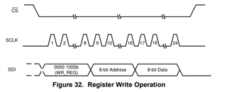
Then, I tried to test read and write command of ADS7028, but it seems not respond at all.

(Write test: Set all channel to GPIO output and set logic 1 , Read test: read several registers ).

Is there any setting of SPI or my process is wrong?

_interrupt void cpu_timer1_isr(void){ // 100us loop 
     if(SPI_STATE==0){
         SpiaRegs.SPITXBUF=0x1000;
         SpiaRegs.SPITXBUF=0x2100;
         SpiaRegs.SPITXBUF=0x0000;
         SPI_STATE=1;
     }else if(SPI_STATE==1){
         SpiaRegs.SPITXBUF=0x1000;
         SpiaRegs.SPITXBUF=0x2100;
         SpiaRegs.SPITXBUF=0x0000;
         SPI_STATE=0;
     }
     if(SpiaRegs.SPIFFRX.bit.RXFFST!=0) Result= SpiaRegs.SPIRXBUF;
}


void SPI_Init(){
    SpiaRegs.SPICCR.all =0x07;  // 8-bit char bits
    SpiaRegs.SPICTL.all =0x06;  // Enable master mode, normal phase, enable talk, and SPI int disabled.
    SpiaRegs.SPIBRR = 0x0016;   // BAUD= LSPCLK/(SPIBRR+1)=  SPIBRR=(LSPCLK/BAUD)-1
    SpiaRegs.SPICCR.all =0x87;  // Relinquish SPI from Reset
    SpiaRegs.SPIPRI.bit.FREE = 1; // Set so breakpoints don't disturb xmission
}

void SPI_FIFO_Init(){
    SpiaRegs.SPIFFTX.all=0xE040;
    SpiaRegs.SPIFFRX.all=0x2044;
    SpiaRegs.SPIFFCT.all=0x0;

    SpiaRegs.SPITXBUF=0x0800;
    SpiaRegs.SPITXBUF=0x0500;
    SpiaRegs.SPITXBUF=0xFF00;
    while(Inter<1000000)Inter++;
    Inter=0;
    SpiaRegs.SPITXBUF=0x0800;
    SpiaRegs.SPITXBUF=0x0700;
    SpiaRegs.SPITXBUF=0xFF00;
    while(Inter<1000000)Inter++;
    Inter=0;
    SpiaRegs.SPITXBUF=0x0800;
    SpiaRegs.SPITXBUF=0x0900;
    SpiaRegs.SPITXBUF=0xFF00;
    while(Inter<1000000)Inter++;
    Inter=0;
    SpiaRegs.SPITXBUF=0x0800;
    SpiaRegs.SPITXBUF=0x0B00;
    SpiaRegs.SPITXBUF=0xFF00;
    while(Inter<1000000)Inter++;
    Inter=0;
}

  • Hello,

    The ADS7028 supports RMS and ZCD, but only one channel at time for each function. For example, you would like use two analog input channels, say CH0, and CH1,  to measure the RMS, you will need to measure channel 0, and then write to the RMS register and change from CH0 to CH1, and then measure the RMS. 

    This would apply the same to ZCD. ZCD can only monitor one input channel. 

    the screen shot you provided is the first frame needed to read a register, in your case you are reading the high threshold for channel 0. But, you are missing the second frame where the register data will be outputted. The register data will not be outputted in this same frame. 

    As for a read test, I suggest not reconfiguring all the channel. you can simply read a known register, such as the System status register. 

  • Hi

    Thanks for replying and clarifying this.

    After re-modifying my code, the current results are as follows:

    After turning on the power, I send two identical frames to read the System status register repeatedly (100uS interval).

    But “MOSI(SDO)” still has no signal output(should I get 0x81?).

    Is there anything I misunderstood?

  • Sorry for the typo.
    Should be *MISO(SDO)*

  • This device by default uses SPI Mode 0, which means that the device "reads" the data on the rising edge of SCLK. Data should change states on the falling edge of SCLK. This applies to both SDI and SDO. 

    When reading System Register, the command 0x81 is valid. I also suggest writing to a register, example the General_CFG register, and then reading back that register to confirm it is configured as you expect.

    -Cynthia

  • Hi

    Thanks for replying again.

    I think there is no problem with my frames now (I send it repeatedly), but there is still no response.

    If you think my current SPI frames settings are correct (polarity, phase, baud rate, etc.), I will replace the chip or get a relevant development board (ADS7038Q1EVM-PDK) for further testing.

    Thanks!

  • you are not counting your clock cycle correctly, you are starting off wrong. one clock cycle should be considered as falling edge to falling edge. in the first clock cycle, the CS falling frame can be considered as the first SCLK, and the first frame then ends with the falling edge, where you currently have part of sclk pulse 2. 

    this means you likely will need to move your commands over one clock cycle.  

    Note the clock numeration in the below image

  • Hi

    After reading F2806x TRM(https://www.ti.com/lit/ug/spruh18h/spruh18h.pdf?ts=1639448638768) for a while, I found this figure.

    This figure shows the mode of SPI-00 (Rising edge without delay) change states on the rising edge and latch data on the falling edge of SCLK, which makes me a little confused with your previous reply.

    SO, I tried two modes and the screenshots are shown below.

    And the ADS7038Q1EVM-PDK I bought last week has arrived

    I use a logic analyzer to monitor its frame, results as shown in the figure below.

    It seems to be different from the above two tests.

    I will try to set the SPI to “Rising edge with delay”, which is the most similar to the package of the development board.

  • In the two test you performed, both will not work with the device in mode 0. The first test, you are still using the wrong edges. You should be "reading" or latching the data on the rising edge of SCLK. Data should change states on the falling edge of SCLK. you are doing the opposite

    The second test, you are using the wrong clock polarity. the clock should be low when idle.  

    The logic analyzer shows the SDO data changing states on the falling edge. Also note that the logic analyzer will use the user-configured mode to read data, it does not know automatically what mode to use. This is a user configuration. From the logic analyzer, you can see that clock polarity is low (0) coming from the EVM, thus your test 2 will not work with the device in Mode 0. 

    To properly communicate with the device and read data as expected, the Clock should be low when idle, latch the data on the rising edge of SCLK., change states on the falling edge of SCLK. and use falling edges to count clock cycles.  This would be "rising edge with delay" in the snippet you shared. 

    Regards

    Cynthia