This thread has been locked.

If you have a related question, please click the "Ask a related question" button in the top right corner. The newly created question will be automatically linked to this question.

DAC38J84EVM: DAC PLL out of lock

Part Number: DAC38J84EVM
Other Parts Discussed in Thread: TI-JESD204-IP, LMK04828

Dear Ti.

I'm using xilinx FPGA kcu040 kintex ultrascale trying to drive the DAC38J84EVM, all pins should have been assigned properly.

I have tried both TI-JESD204-IP and XILINX JESD204 IP.(When I'm using TI-JESD204-IP, I blocked the adc out put and adc input).Both design finally came out with the same "DAC alarm" ---DAC PLL OUT of LOCK.

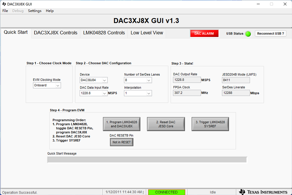
My configuration is:
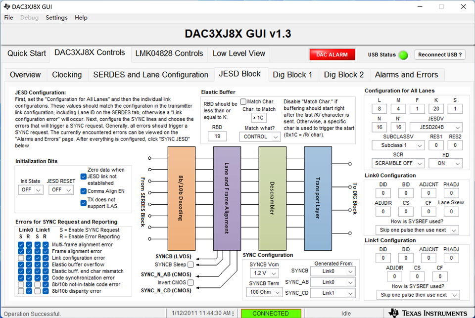
LMFS: 8411
sample rate: 1228.8MSPS,
interpolation: 1
Other detailed settings are automatically generated by the Quick start page following the  DAC3XJ8XEVM guide book's  chapter 4.3 'DAC3XJ8X Quick-Start Procedure'.

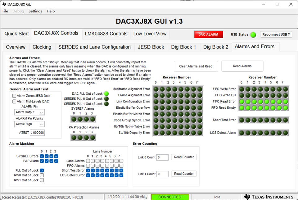
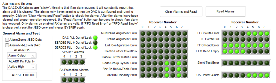
The ALARM and Errors page:

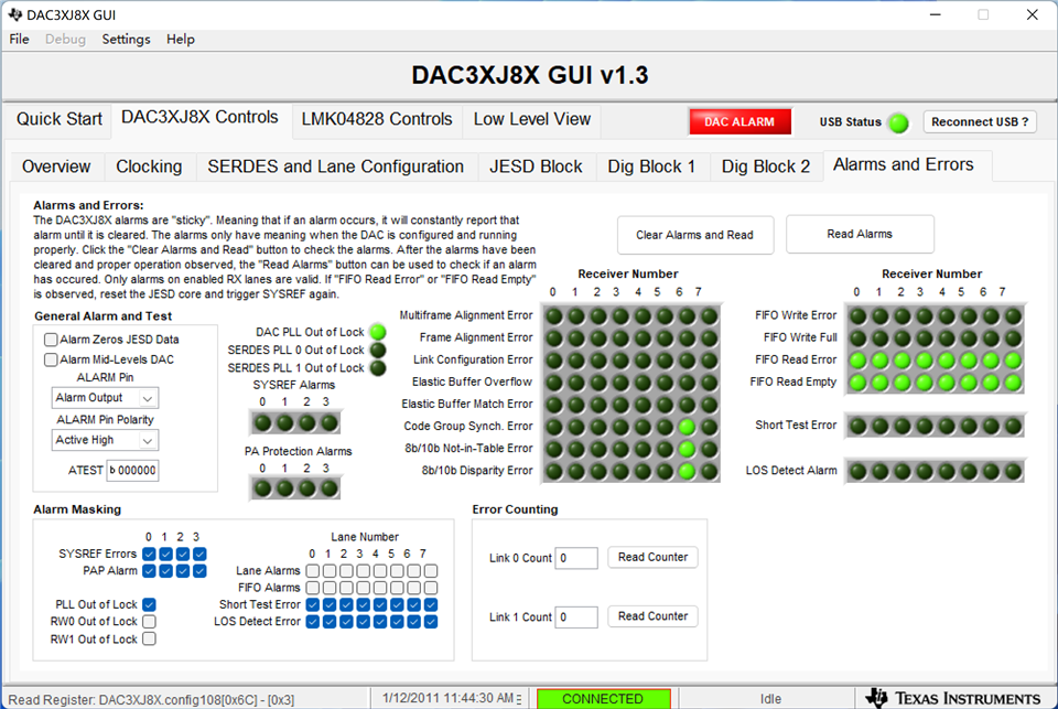
Here is my cfg from 'Low Level View' Page:cfg.cfg.

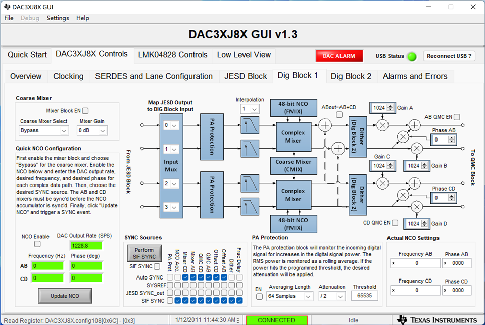
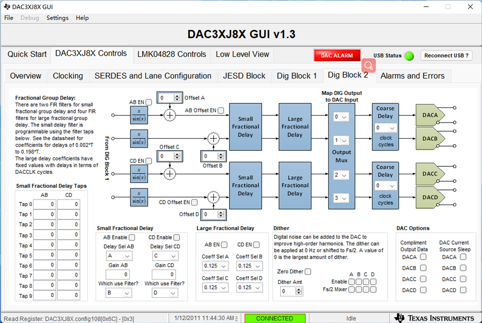
some detailed settings:

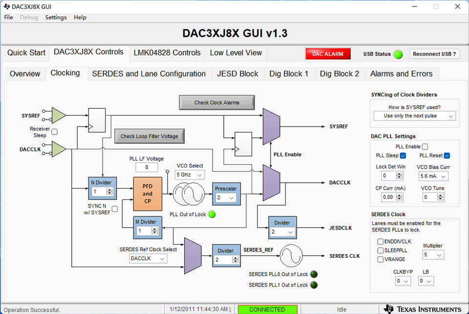
I have searched some posts in the forum, but their configuration is not quite the same as mine. I tried to follow some posts, but failed.It seems I have to set pll_vcosel,pll_vco...But I didn't find where and how to set there parameters correctly

Please help me to config the settings.

  • Shuai,

    It appears you have either a bad serdes lane (#6) which could be due to an assignment error, or a timing issue with the FPGA (since you are seeing FIFO errors).  With the setup you are showing, the FPGA is receiving a 307.2MHz reference clock. Make sure this is what the firmware is expecting. If there is a possible issue with lane 6, try using the 4 lane approach shown in the attached file. You can also try the original 8 lane mode but with a reduced serdes rate to see if this helps. This mode is also shown in the attached file.

    Regards,

    Jim

    DAC38J84_LMF_4421.pptx 

  • Dear jim

    I've re-timing my program,making sure there is no timing issue in my program.
    now the possible issue with lane 6 is no longer exist ,but the DAC pll is still out of lock,and the FIFO read error and FIFO Read Empty is still on.


    What should I check now?(Sorry for those problems)

    Thanks a lot

  • You are not using the DAC PLL so this is normal. I think the FPGA is having issues and you should contact Xilinx for help. If you use Chipscope, you should see the FPGA sending valid data after CGS has completed and the SYNC staying high. Double check the FPGA JESD parameters and make sure they are matching the DAC parameters. Is your FPGA expecting two clocks (core clock and reference clock) from the DAC EVM or one?

  • My test bench block diagram is above.
    Input from DAC38J84EVM are:
    sync0_p/n connecting  SYNCBP/N port (DAC),
    refclk_p/n connecting  DCLKOUT0p/n port (LMK04828 , 307.2MHz),
    sysref_p/n connecting SDCLKOUT1p/n port (LMK04828 , 307.2MHz)

    data output to DAC are:
    tx_p/n[7:0]. those are GTH transceiver, connecting according to the schematics.

    I'm confused about those clocks.It seems that the frequency of refclk is set in the jesd204 ip, and sys_ref is 1/40 of line rate and set in the GUI.
    I have tried ILA ,I found sometimes the sync_signal is low.

    Is there any thing wrong?Or what should I do for further debugging?

  • Max SYSREF = data rate / (K * N) where N is any whole integer. In your setup, the max SYSREF can be is 61.44MHz. Give this a try.

  • Sorry,,but how to change the SYSREF individually?in my setup, the refclk and sysref comes from DCLKOUT0 and SDCLKOUT1. I think the refclk is 307.2MHz, and the sysref is also 307.2MHz because in the clock output page, the CLK0 & 1 are controlled by one divider.
    In fact I'm not quite sure how to tune the frequency.

  • I have tried the 4421 configuration.seems the alarms still on.

    What's the most likely problem, the program or the FPGA ,or any thing i should make sure of?

    thanks

  • The FPGA.

  • SDCLK uses the SYSREF divider shown on the SYSREF and SYNC tab. You should have 160 for the default divider (see attached). This will create a SYSREF frequency of 15.36MHz which is fine for your setup.

    4405.SYSREF.pptx

  • Shuai,

    Here is an example project using the TI JESD IP.

    Regards,

    Jim

    TI_JESD204_IP_KCU105_DAC38J84_841.zip 

  • jim

    Thanks for your kind help.Now I will try to work on another FPGA board.


    I want to program the FPGA as a DDS to be  the source of the DAC input data  (rather than simply reading data from the DDR),and using PC to fast tune the frequency and phase of the signal.Further, I hope to sum up several DDS digital signals to synthesize a new waveform.
    The benefit is the data from PC are simplified into a few control commands.


    I think the TSW14J56EVM would be a good starting point,there are 8 lanes and USB 3.0 port. Can I reprogram and modify the TSW14J56EVM to meet my demand? If it is possible, Can I  still use the TI-JESD204-IP or just modify the source code(is there enough logic gate source in FPGA to add my design?)? I'm a little worried about the difficulty to establish the jesd204b link between TSW14J56EVM and DAC 38j84.

    wish to hear your Comments and suggestions.

    Best regards,

    shuai

  • Shuai,

    You can reprogram the TSW14J56 using the JTAG interface. The main problem you might run into is the TI JESD204B IP is currently only for Xilinx FPGA's. The TSW14J46 uses an Intel FPGA. I would suggest you try modifying the provided TSW14J56 source code found on the TSW14J56EVM product folder of the TI website. Depending on your experience, this may be an easy task or a difficult task.  I do not know how much logic gates your application requires so only you can answer this. Since the source code for the TSW14J56 was developed by a third party vendor that no longer supports this, TI will not be able to provide any support with this for you. 

    Regards,

    Jim