


Other Parts Discussed in Thread: DAC3151
Dear Texas Instruments,
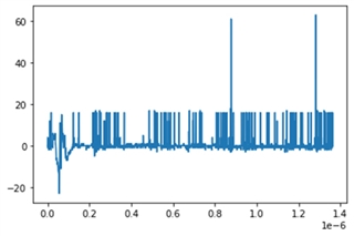
We have designed a circuit with an ADC07D1520 and DAC3151 on an embedded system managed by an FPGA. We are having some problems dealing with the ADC output data. The output from DAC and inputs of ADC are cascaded and we measured the waveform with an oscilloscope at the inputs of ADC and it is fine as we programmed, but the signal acquired by ADC is a bit odd: we get a signal that is non sinusoidal and with a duration much smaller than it should be, for instance this should be a 20 MHz sine wave with 10 cicles. Clearly in the beginning we have a signal, but it fades out right after and does not correspond to 10 cicles of a 20 MHz sine wave.
Therefore, we are contacting you to see if you can help us. In our project, the mainly ADC07D1520 configurations are:
- Double Data Rate (DDR) enable operating at 1.5 GHz;
- only one DCLK with 90º Phase;
- Demultiplexed Mode;
- Dual Edge Sampling (DES) mode with I-channel operating by both ADCs.
We are using a Xilinx ZYNC-7000 FPGA, model Z-7010, to manage the ADC data sampling. The interface between the ADC and the FPGA is described as follows:
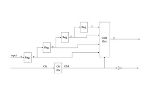
- Each differential ADC OUTPUT P and N pair was mapped with Differential Input Buffer Primitives (IBUFDS) from the Xilinx library, including the DCLK applying a specific clock differential input buffer (IBUFGDS). In the figure below, the Input Buffers are the Qd, Id, Q, I, and Clk modules. The Clk Up and the Clk Dn modules are latches to store the P and N concatenated values, respectively stored by the rising and falling Clk edges. The output Data signal is the concatenation of P and N sampled values.

The subsequent circuit is a serializer module to concatenate four Data consecutive values. It was developed a latch cascade structure to shift the consecutive Data values, and the Data Out signal is stored considering a clock signal (Clk4) with one-fourth of the DCLK frequency.
We also use the DCLK_RST pins to sync the converter with our DAC so that both converters have a common reference frame. On the DAC there was an error on hardware and the pins got connected wrong, so we use the sif_sync feature to sync the converter as we drive the DCLK_RST on the ADC. Could it be a mistake on the use of this feature?
Regards, Willian.
