This thread has been locked.

If you have a related question, please click the "Ask a related question" button in the top right corner. The newly created question will be automatically linked to this question.

AFE58JD48: Data converters forum

Part Number: AFE58JD48
Other Parts Discussed in Thread: AFE58JD28

Dear Support:

Now I am using FPGA(XCKU3P) to receive sampling data from AFE58JD48 through JESD204B.

The AFE configuration is JESD 160X Mode, Subclass2, 16bit-30MHz sampling rate, which is configured by SPI according to the following process:

0x12 0x000A //PAGE_SEL_8CH_DIG1, PAGE_SEL_8CH_DIG2 = 1

0x31 0x00C0 //PLL_MODE = 160X, CTRL_K=1, CTRL_MODE = 1

0x32 0x8000 //EN_1L_MODE0 = 1

0x34 0x1107 //JESD_SUBCLASS = 2, JESD_VERSION = 1, K = 8

0x35 0x00C0 //L=1, CTRL_L = 1, CTRL_M = 1

0x36 0x0003 //M = 4

0x5D 0x8000 //EN_1L_MODE1 = 1

0x2C 0x0008 //EN_1L_MODE2 = 1

0x30 0x8002 //Enable Mux Pdn. Mux_Pdn_3_4; Bring Lane3 on Lane2; Pdn JESD2 (for Top ADC)

0x30 0x8006 //Mux_Pdn_5_6;Bring Lane5 on Lane8;Pdn JESD1(for Bottom ADC)

0x12 0x0000 //Disable Page Select

0x12 0x0002 //PAGE_SEL_8CH_DIG1 = 1, Selecting Top 8 channel

0x5F 0x00A0 //Pdn Lane 2

0x12 0x0008 //PAGE_SEL_8CH_DIG2 = 1, Selecting Bottom 8 channel

0x65 0x0050 //Pdn Lane 7

0x12 0x0000 //Disable Page Select

FPGA firmware Use Xilinx IP JESD204(7.2),1-Lanes,8-F,8-K,4.8Gbps-LineRate。

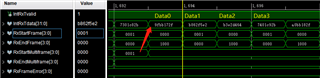
The Bit file is generated and downloaded to FPGA, and rx_data is obtained through ILA. I want to know how to convert rx_data into sampling data of each channel.

  • Hi Chengan,

    Let me have a look at the sequence and settings you are programming. I will let you know the data separation logic on the CML lanes.

    Quick question, are you using demodulation as well?

    Regards,

    Abhishek

  • Hi Chengan,

    As per your settings, you are using CML_lane1 and CML_lane 8. 

    You can refer to table 62. Frame assembly with Demod Disabled in the datasheet.

    You should receive data in the following manner:

    On lane 1 : D11, D21, D31, D41 | D51, D61, D71, D81| D12, D22, D32, D42| D52, D62, D72, D82 |.... and so on

    On lane 8: D91, D101, D111, D121 | D131, D141, D151, D161 | D92, D102, D112, D122 | D132, D142, D152, D162 |... and so on,

    where

    Dxy stands for data of channel x at instant y; x = {1:16}; y = 1, 2 and | represents frame clock

    Hence the data in this format is being received by the FPGA IP, which after 8b/10b decoding I think is shown in your ILA. iNTRXTDATA  which is 32 bit is showing two consecutive channels data.

    Can you program known data/ test pattern into the device, which can help further to decode it.

    Let me know if you have further question.

    Thanks

    Abhishek

  • Hi Chengan,

    Looking at the ILA capture you have shared, I think something is wrong because RxStartFrame signal if you look, is toggling every consecutive cycles which is 1, 0, 1, 0... and so on.

    Ideally it should be 1, 0, 0, 0, 1, 0, 0, 0, 1... every 4 cycles.

    The main reason for it is that the deserializer in the FPGA runs at 40x and the transmit is happening at 160x. So you need to have 4x Fs faster clock on the FPGA.

    Based on above I want to confirm the following:

    1. Are you giving 4x faster clock i.e 120 MHz clock to FPGA.

    2. on the FPGA IP, i.e. receive IP, the value of F programmed should be 4. (you are programming 8)

    3. The valid data on the  will come after the signal IntRxTvalid becomes high. The rising edge on the IntRxTvalid signal will start valid data on the IntRxTdata which will be D1, D2 (32 bit)), [D3, D4], [D5, D6], [D7,D8],...

    4. The RxStartFrame will follow 1 [during D1, D2], 0 [during D3,D4], 0 [during D5,D6], 0 [during D7,D8]

    Let me know if my explaination is not clear.

    Regards,

    Abhishek

  • Hello, I'm sorry it took so long to reply to you.

    I have solved this problem.

    According to the following figure (timing diagram of JESD204B transmission in AFE58JD28 106X mode), one frame of AFE data (D1+D2+D3+D4 or D5+D6+D7+D8) has a total of 64bit, while one Lane of XilinxJESD has a width of 32 corresponding to rx_data, so two XilinxJESD rx_data are needed to transmit one AFE frame. That is, four consecutive rx_data are needed to complete the transmission of D1+D2+D3+D4+D5+D6+D7+D8 data.

    Restore rx_data data according to the above information:

    When the StartMultiframe=1, the next four data are DATA0[31:0], DATA1[31:0], DATA2[31:0] and DATA3[31:0], then:

    CH1={ DATA0[7:0],DATA0[15:8]}
    CH2={ DATA0[23:16],DATA0[31:24]}
    CH3={ DATA1[7:0],DATA1[15:8]}
    CH4={ DATA1[23:16],DATA1[31:24]}
    CH5={ DATA2[7:0],DATA2[15:8]}
    CH6={ DATA2[23:16],DATA2[31:24]}
    CH7={ DATA3[7:0],DATA3[15:8]}
    CH8={ DATA3[23:16],DATA3[31:24]}

    In this way, every four data groups can obtain the sampling data of eight channels (here, taking lane1 of AFE as an example).

  • Hi Chengan,

    Good to know that you are able to resolve the issue. I am closing this thread, please feel free to reach out if you need any other information.

    Thanks & regards,

    Abhishek