This thread has been locked.

If you have a related question, please click the "Ask a related question" button in the top right corner. The newly created question will be automatically linked to this question.

DAC5670-SP: Pin configuration

Part Number: DAC5670-SP

Hello E2E,

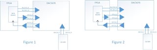
Can we leave DTCLK_P/N and DLYCLK_P/M pins floating if they are not used?

Regards,
Carlo

  • Carlo,

    How do you plan to align the input data without DLYCLK? The clock latching the data input internally is 1/4th of the DACCLK frequency, which means it can have up to 4 different phases depending on how the dividers startup. The DLYCLK output has the same phase as the data latching clock, so the data timing (setup and hold times) are relative to DLYCLK (or you can use DTCLK and the DLL, in which case DLYCLK is optimally delayed for the best timing for the data). If you do not use DLYCLK, you will need to generate a divide by 4 clock externally that will  have no relationship to the internally divided clock.

     DTCLK can be left floating if the DLL is not used, but highly recommend that you use DLYCLK.

    Regards,

    Jim

  • Hello Jim,

    Please see the response of our customer as follows. Do you have an example or app notes on how to use the DLYCLK ? Is it recommended to use the DLL in order to align data? I am designing a board that interfaces with another board that controls the DAC through an FPGA. So it seems like I have to connects the DLYCLK to the FPGA in order for the FPGA designer to use the DLYCLK to align data?

    Regards,
    Carlo

  • Carlo,

    The only thing I can offer is for the customer to follow what is shown in Figures 1, 2 and 15 of the data sheet along with section 8.3.2

    . It is recommended to use the DLL, especially if running at the max sample rate. The TE EVM routed this signal to the board connector which then went to the FPGA on the pattern generator board used to test the EVM. If interested, we can send the DAC5670EVM design files.

    Regards,

    Jim 

  • Hello Jim,

    Thank you for the suggestion.

    The functional BLK diagram on sheet 15 shows on die termination on the data and DTCLK inputs but not on the DACCLK inputs. Does this mean the DACCLK inputs need the termination external to the DAC5670? And what is the outputs impedance of DLYCLK outputs? Is this a high impedance outputs and so we need to add termination to this

    Regards,
    Carlo

  • Carlo,

    I am looking into this. How does the customer plan on driving the DACCLK and what are they sending the DLYCLK to (what type of load/device)?

    Regards,

    Jim

  • Carlo,

    The customer should use an external 100 Ohm termination resistor across DACCLKP/N and place as close as possible to the DAC.

    DLYCLK has two modes selected by the LVDS_HTB pin. If using LVDS mode, DLYCLK will swing between 900 and 1400mV (this would be each side to 50Ohm load). If using HTB mode, the swing would be 450 to 700mV. 

    Regards,

    Jim

  • Hello Jim,

    Our customer is limited on IO pins on the FPGA, here is a configuration they can do that would use 100% of the available pins. Or is there another configuration they can do with a total of 22 pins? This uses 20 for the data only driving 13..4 and 2 for the DLYCLK and DTCLK.

    DAC5670 DATA CLK CONFIG.pdf

    Regards,
    Carlo

  • Carlo,

    The whole point of DTCLK is that is has the same exact timing as the rest of the data – it is simply a bit toggling 1 0 1 0 1 0. The edges need to be time aligned to the edges for the rest of the data, so when the DLL optimizes the DLYCLK timing by measuring DTCLK, the rest of the data also has the right timing.

     We suggest the customer to give up one more LSB and use the pins for a differential DTCLK. We don’t think they will see a significant performance difference for not having the extra LSB.

    Regards,

    Jim

  • Hello Jim,

    Do you recommend using 9 bits with the internal diff TX/RX from the FPGA over using 10 BITS and external Diff RX/TX. So BLK diagram 2 over BLK diagram 1?
    Regards,
    Carlo

  • Carlo,

    Yes, we recommend using 9 bits with DTCLKP/N used as a differential pair. There was no block diagrams attached.

    Regards,

    Jim

  • Hello Jim, here is the attachment

    1258.DAC5670 DATA CLK CONFIG.pdf

    Regards,
    Carlo

  • Yes, Figure 2 is what we recommend.