This thread has been locked.

If you have a related question, please click the "Ask a related question" button in the top right corner. The newly created question will be automatically linked to this question.

DAC5688: What would be the root cause of the abnormal output?

Part Number: DAC5688

Hello,

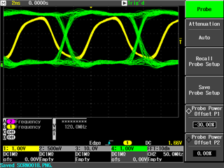
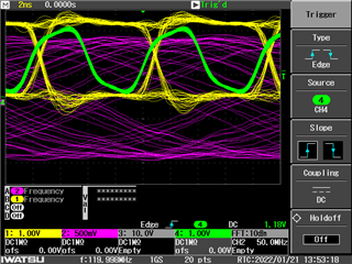
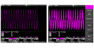
My customer uses DAC5688 on their own board.  They sometimes get good waveform as shown lower left, but they sometimes don't do as shown lower right.  Would you please tell me what do you suppose the root cause would be?

When they get the right one, it returns to normal only when they do hardware reset or PLL_sleep(CONFIG26 0x0d -> 0x0e -> 0x0d).  I mean when they get good one, they can keep it unless they do hardware reset or PLL_sleep.  When they get abnormal one, they can't make it to good one unless hardware reset or PLL_sleep.

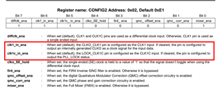
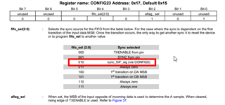
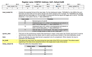
These are the register settings.

Addr. Data
0x04 0x00
0x05 0x80
0x06 0x00
0x07 0x00
0x08 0x00
0x09 0x00
0x0A 0x00
0x0B 0x00
0x0C 0x00
0x0D 0x00
0x0E 0x00
0x0F 0x24
0x10 0x00
0x11 0x00
0x12 0x00
0x13 0x00
0x14 0x00
0x15 0x00
0x16 0x15
0x17 0x00
0x18 0x80
0x19 0x00
0x1A 0x0D
0x1B 0xFF
0x1C 0x00
0x1D 0x18
0x1E 0x13

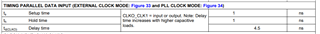
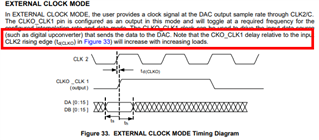
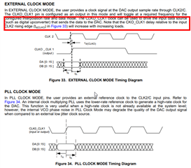
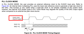
Note that they don't use complex mixer.  Note also that they confirmed the recommended startup sequence shown on page 45, the timings(PLL clock mode) and clock input(CLK2/CLK2C) shown on page 7.  Nothing seems wrong, but it sometimes doesn't work well.  I'd like to know the reason why it is.

Best Regards,

Yoshikazu Kawasaki

  • Hello,

    Please advise the condition for the CLKO_CLK1 state

    With PLL mode, the CLKO_CLK1 state can be input or output. Since I did not see register 0x02 being configured, most likely the CLKO_CLK1 is configured as output.

    If this is the case, please advise the Data[15:0] CMOS GPIO setup/hold time with respect to the CLKO_CLK1 output. 

    Please advise if it is possible to provide timing diagram to ensure good setup/hold time with respect to the CLKO_CLK1 output

    Please also try to reduce the load for CLKO_CLK1 output. If there are too much capacitance on the line, the delay will become significant and cause bit errors

  • Hello Kang-san,

    Thank you very much for your quick reply.  I should tell you that my customer only uses CLK2 and CLK2C since they don't use dual clock mode.  Even in this case, do they have to configure CLKO_CLK1 as well?

    Best Regards,

    Yoshikazu Kawasaki

  • Kawaksaki-san,

    Yes, CLKO_CLK1 either need to be input or output. Regardless of the IO status, setup/hold time must be followed. 

  • Hello Kang-san,

    They confirmed the CLKO_CLK1 was configured as output as you mentioned and the timing was no problem as attached(Ch1:CLKO_CLK1, Ch2:DA3, but the other data pins are almost the same, so there is no setup/hold timing issue here).  CLKO_CLK1 pin is floating on their board, so there is almost no load there.  What should they do next?

    Best Regards,

    Yoshikazu Kawasaki

  • Hi Kawasaki-san,

    If it is floating, then how is the relationship of the data generated with respect to the CLKO_CLK1? The CLKO_CLK1 is typically connected to host to provide the reference to generate the data stream

    Please also try to toggle SIF_SYNC via writing 0->1->0 of the config5 SIF_SYNC Bit. This is the default to sync the FIFO.

    Currently the FIFO is set to be synchronized by rising edge of the TXENABLE. The customer may also try to set TXENABLE from logic low to logic HI again to initialize the FIFO to see if the issue can be resolved. 

  • Hello Kang-san,

    Thank you very much for your quick reply.

    Thanks to your advice, they found when the output became abnormal.  Since as you mentioned, they can't control the timing between the data and CLKO_CLK1 output because it's floating, so the data sometimes has timing violation depending on the phase of CLKO_CLK1 output.  Would you please tell me how they can control the phase of CLKO_CLK1?  Or do they have to connect CLKO_CLK1 to the host to control the timing of the data?  You mentioned typically, so I expect DAC5688 to control the phase of CLKO_CLK1 even though I can't find such a register bit.

    Best Regards,

    Yoshikazu Kawasaki

  • Hello Kawasaki-san,

    The CLKO_CLK1 is the "DATA Clock" used to latch the input CMOS data stream. Therefore, either the customer has to use the CLKO_CLK1 as an output from the DAC5688 to the input of the FPGA for "reference" of the setup hold time, or the customer can configure the CLKO_CLK1 as an input

    If CLKO-CLK1 is an input, the customer can have another CMOS GPIO from the FPGA as "DATA clock" to latch the CMOS data. This can ensure good setup/hold time. 

    The only other phase control of the CLKO_CLK1 is the inverting function. However, this only create 180 degree offset to allow better setup/hold time margin. This does not ensure synchronicity of the clock/data relationship

  • Hello Kang-san,

    Thank you very much for your quick reply again.

    I understand my customer can fix this timing issue by configuring the followings.  Am I correct?

    1. CLKO_CLK1 as input.

    2. Both CLKO_CLK1 and data from FPGA

    Best Regards,

    Yoshikazu Kawasaki

  • Hi Kawasaki-san,

    Yes, you are correct. This is one way to ensure CLKO_CLK1 can have proper setup/hold time with respect to the data input. Thank you.