This thread has been locked.

If you have a related question, please click the "Ask a related question" button in the top right corner. The newly created question will be automatically linked to this question.

DAC38J84: DAC Full-scale output range

Part Number: DAC38J84

Hi,

I am currently doing a test on DAC38j84EVM with CW tone (no data input) and defining the link budget analyse @2.4576 GSPS.

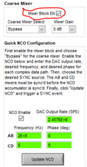
So with 2 transformers on EVM board (impedance ratio: first one 2:1 and second one 1/1), with settings for coarse gain=15, NCO actived and mixer gain=0dB, const value=0x0000, offset bninary, internal reference, I got on spectrum analyser (50Ohm) about 0dBm to -2dBm for f<300MHz and -3dBm to -4dBm for [400MHz, 1GHz]. 

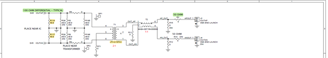
I see the Rbias=1.91kOhm on schematic of the EVM board, I chose the internal reference which should be 0.9V, so theoretically the Iout ma will be (0.9V/1.91kOhm)*64=30mA. With this current and with 50Ohm shunt resistor at output of DAC on the EVM board I may have 1.5Vp-p at the first transformer input and 1.06Vp-p on the 50Ohm output which leads to about 4.5dBm.

I don't know why there is so much loss (cascaded transformers IL should be within 2dB according to datasheet). Could you explain this pls ?

Another two small questions: 

1. The first transformer JTX-2-10TA+ from Minicircuit is for 75Ohm system and I would like to know why use this 75Ohm transformer instead of a 50Ohm transformer ?

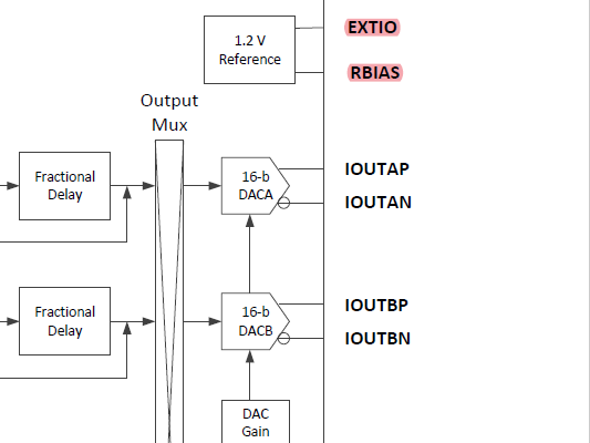
2. On the block diagram of the DAC38j84 datasheet the reference is 1,2V instead of 0,9V, why ?

Thanks in advances for your help,

Best regards,

Xin

  • Xin,

    There is a 6db loss due to the mixer. This is why there is an option for 6db of digital gain to be added. This is why you are seeing this loss. Bypass the mixer and you will see the output power increase.

    1. The impedance of the balun or transformer is not so critical, you can always re-match the impedance as needed for the circuit to work appropriately. This part was chosen for its wide pass band.

    2. This is an error in the data sheet. This should be 0.9V.

    Regards,

    Jim

  • Hi Jim,

    Thanks for your reply.

    So with the current configuration with mixer gain=0dB, you mean I have a lower DAC output current which is still lower than the 30mA FS current? or this will result a lower FS output current? 

    When you mean bypass do you mean I need to bypass the coarse mixer or I just need to disable the NCO ( the signal from FPGA still go through the Full complex mixer)? I used full complex mixer and the coarse mixer is bypassed as like attached photo. How to bypass the full complex mixer? So I need to disable the Mixer Block EN to bypass all mixers ?

    Regards,

    Xin

  • Xin,

    To bypass the mixer and NCO, you would just not enable them in the GUI. The mixer gain does not set the 30mA FS current. This is set by the external Rbias resistor.

    The digital output after the mixer has an option to go directly to the DAC or through a divide by 2 block. If the divide by two logic is not used (Mixer Gain 6 dB), if there is a complex fullscale tone at the DAC input, you will get a fullscale tone at the output of the mixer.

    However, a complex fullscale tone is not the highest power possible at the input. If you go to the corner for example, 32767 + j*32767, you will have 3dB higher input power and this saturates the mixer (you could have this case for a modulated signal). To prevent saturation, the data has an option to go through a divider with 6dB lower power (Mixer Gain 0 dB), basically the data shifted down by 1 bit. This is not optimum as you will never be higher than -3dBFS at the DAC output, but it basically comes for free. An optimum backoff of 3dB would cost more power and circuit size.

    Regards,

    Jim