This thread has been locked.

If you have a related question, please click the "Ask a related question" button in the top right corner. The newly created question will be automatically linked to this question.

ADS8924B: Question about ADS8924B

Part Number: ADS8924B

Hello:

At present, we are using FPGA to access the internal register of ADC chip and read and write it. We need to consult you with the following questions:

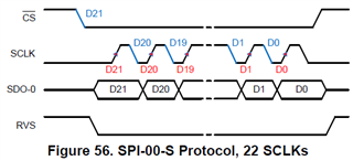
1、During the read operation, the host (FPGA) will first send the read instruction and wait for it to be sent, and then send an NOP instruction. While sending the NOP instruction, the host receives the data from the ADC chip. Is the above reading process correct?

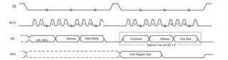
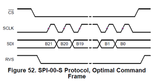
2、In combination with relevant timing requirements, the timing of SPI interface I designed is as follows,Is the design correct?

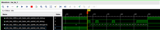
3、To access the data inside the ADC chip_ Take cntl register as an example, address = 010h, write its value as 0x0f, and send a write instruction: 0x24100f. The actual SPI interface timing is shown in the figure below:

Read data for_ For the value in cntl register, first send the read instruction: 0x221000, and then send the NOP instruction: 0x000000 after the read instruction is sent. The actual SPI interface timing is shown in the figure below:

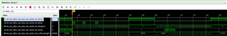
If the operation is correct, should the read value be 0x22100f? Is the timing design of the above interfaces correct?

4、If I want to read the data result after ADC chip conversion, I will first pull up the convst signal for 35ns, and then pull it down. After the RVs signal is pulled up, I start to send a NOP instruction and read out the converted data at the same time. Can you read the correct conversion data according to the above process?

I hope you take the time to have a look, thank you!

REF1: ADC chip model ads8924b.

Ref2: SPI timing protocol I use the power on default configuration spi-00 format, X1 mode, and the clock frequency is 40MHz. I send data on the falling edge of the clock and collect data on the rising edge.

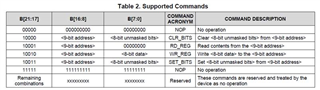
ReF3: the definition of ADC chip instruction format is shown in the following table:

  • Hello Jimmy,

    1. Yes, that is the correct sequence.  Here is an example timing diagram.

    2. Yes, this appears to be correct as long as all timing requirements are met.  Please note, for SPI-00-S, the ADS8924B will capture data on the rising edge of SCLK.  In this example, you are sending a WR_REG command to address 0x10h (DATA_CNTL Register), with contents 0x0Fh.  Note that this register sets the parity information.  However, the LSB (Bit 0) selects the contents of the fixed-pattern register when set to 1.  The fixed-pattern is only used for debug, since the ADC will only output the contents of the pattern register and not the ADC conversion result.  In order to read the ADC conversion result, this bit needs to be cleared to 0.

    3. If you want to write the value 0x0Fh to register 0x010h, the following 22b transfer will look as follows:  0x10 0100 0001 0000 0000 1111b 

    Yes, to then read the value in that register, you would send 0x10 0010 0001 0000 0000 0000b.  In the next frame, the first 8b will be the register value, followed by 14 0's.  In this case, you should read 0x00 0011 1100 0000 0000 0000b, which agrees with your attached waveform capture.  The results read in the following frame after a RD_REG command are just the 8b contents of the register, followed by zeros.

    4. Yes, this is the correct process.  As I noted above, the DATA_VAL bit in the DATA_CNTL Register (010h) should be set to 0b to get the conversion result.  In your above example, you have set this bit to 1, which will replace the conversion result with the PATN CNTL register contents, which default to 0x000000h on power-up reset.

    Regards,
    Keith Nicholas
    Precision ADC Applications