


Dear Sir/Madam,
I am using LM98640QML ADC for one of my projects for data acquisition. Here My Video signal Voltage is 1.5 to 4.8V(Black level is 1.4V) we are scaling down to this signal to 0 to 2V by using op AMP .
So our ADC will receive 0 to 2V input signal on OS1+ pin(Non inverting). I am using Sample and Hold mode for data acquiring. Inn datasheet they have given
In Sample/Hold Mode, the DC bias point of the input pin is typically set by actuating the input clamp switch during optical black pixels which connects the input pins to the VCLP pin DC voltage. The signal controlling this switch is CLPIN. CLPIN is an external signal connected on the CLPIN pin.
Taking the average of these signal components will result in a final “clamped” DC bias point that is close to the Black Level signal voltage. To provide a more precise DC bias point (i.e. a voltage closer to the Black Level voltage), the CLPIN pulse can be “gated” by the internally generated CLAMP clock.
But In datasheet then have mentioned CLPIN for CDS mode in fig17 & 18.
So what will be the CLPIN function in S/H mode . PFA of my circuit.
It well be very useful for me and application if anyone explained deeply on this topic.
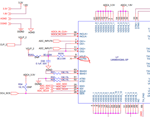
I have connected My i/p signal to OS+ pin and vclp to OS-. . CLPIN pin kept it as open.
My question is to set a bias point , do i need to connect any ref voltage level on CLPIN pin or Can it be generated by BIT register configuration ?
VCLP pin to be connected to OS- I/P ?
Thanks in Advance
