This thread has been locked.

If you have a related question, please click the "Ask a related question" button in the top right corner. The newly created question will be automatically linked to this question.

ADS8422: Circuit of input stage for ADS8422

Part Number: ADS8422
Other Parts Discussed in Thread: THS4131, , THS4551, ADS9224R

Hello,

I considering AD conversion circuit that circuit is used ADS8422 and THS4131.

I considering this circuit based on figure 29 of ADS8422 data sheet.

Input voltage range of this circuit is +10V to -10V and sampling rate is 3MHz.

I want to confirm that there is no problem with the circuit changes shown below.
I would be happy if you could tell me anything wrong with the circuit operation.

<Point of change>

1. Change the resistance combination to 2200 ohm and 390 ohm to get a gain of 0.18 for THS4131.

2. Connect +10V/-10V input signal to +VIN of figure 29.

3. Connect GND(0V) to -VIN of figure 29.

4. Add 560pF capacitor parallel with each 390 ohm resistors. (700kHz anti-aliasing filter for sampling rate 3MHz)

5. Supply +5V power and -5V power to THS4131.

6. Supply +5V power to ADS8422.

Regards,

MESH

  • Hello,

    You can use the THS4131 to translate +/-10V single ended input to the input range of the ADS8422.  I assume you are using the internal 4.096V reference, which results in a full scale input range of +/-4.096V differential.

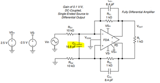
    1.  Using 2200ohm and 390 ohm will provide a gain of 0.18.  With a +/-10V input, this will result in an output range of +/-1.8V, which will not take advantage of the full scale input range of the ADC.  You could use 1200ohm and 390ohm, which will result in an output of +/-3.25V. and still leave output voltage headroom for the THS4131 (+/-3.6V minimum when using +/-5V supplies)

    2.  Yes, the THS4131 can translate a single-ended +/-10V to the proper differential voltage for the ADS8422 inputs.

    3.  Yes, connect to ground for a single-ended input.

    4.  Yes, this can be done to provide an anti-alias filter.  I suggest adding an additional capacitor between the inverting and non-inverting inputs (pins 1 and 8) of the THS4131 as a place-holder for frequency compensation.  If needed, this capacitor value is typically 4x the feedback capacitance, or 2.2nF.  For details on why this capacitor is needed, please refer to the THS4551 datasheet, section 10.1.6 (Designing Attenuators)

    5.  +/-5V supplies will provide voltage headroom for the inputs.  However, the maximum output voltage with +/-5V supplies is limited to about +/-3.6V, which will limit the full scale range of the ADS8422 using a 4.096V reference.  Also, if there is a fault and the output of the THS4131 swings to the negative supply rail (about -4V), the inputs to the ADS8422 could be damaged.  If using the THS4131, I suggest adding some type of diode clamp to the amplifier output to limit the negative voltage to about -0.7V.

    With the addition of the frequency compensation capacitor, and adjusting the gain resistance to 1200ohm, you can maximize the performance of the amplifier and ADC.  However, I suggest using the THS4551 amplifier.  This is a newer device, and can operate from a single +5V supply.  This will result in lower power dissipation, and if there is a fault, the outputs will be limited to the ABS maximum input voltage range of the ADS8422.

    Also, since you are operating at 3MHz, you may want to consider the ADS9224R.  This ADC can operate at a maximum sample rate of 3MHz, and also includes an internal reference, providing a full scale input range of +/-4.096V.  The ADS9224R is a much newer device, and we also have an evaluation board.

    Regards,
    Keith Nicholas
    Precision ADC Applications

  • Hello, Keith Nicholas

    Thank you for your reply.

    I will use 1200 ohm / 390 ohm and additional capacitor.

    And I will consider THS4551 and ADS9224R.

    Thank you very much.

    Regards,

    MESH

  • Hello MESH,

    You are welcome.

    Regards,
    Keith