This thread has been locked.

If you have a related question, please click the "Ask a related question" button in the top right corner. The newly created question will be automatically linked to this question.

ADS1234: I made a custom development board. I am not able to get it to work properly

Part Number: ADS1234

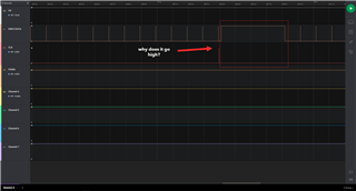
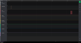
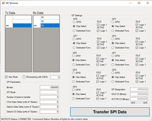
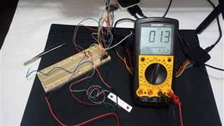
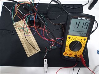
Based on the previous post https://e2e.ti.com/support/data-converters-group/data-converters/f/data-converters-forum/1037254/ads1234-minimum-circuity-to-get-it-working/3850194?tisearch=e2e-sitesearch&keymatch=%20user%3A498854#3850194 I am having trouble getting this to work properly.

A video showing the issue is at this link: https://ticsc.service-now.com/sys_attachment.do?sys_id=8228a303973d059082c3348c1253af73

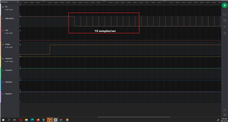
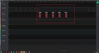
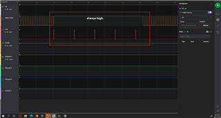
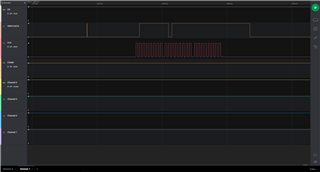
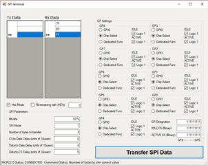
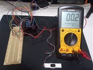
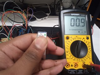
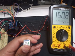
Basically the readings are always showing 255. It is not working as expected.

Thank you so much for your help.

  • Hi Anthony,

    Unfortunately I could not access the video, so I don't know what you are attempting to show me.  First start out with the basic supply and pin settings.  Measure each device pin of the ADS1234 with a voltmeter and make sure that there are no floating digital pins.  The most common mistake is to leave one of the pins floating or to have PDWN low (which powers down the device) instead of high (making it active).

    If you have access to an oscilloscope of logic analyzer, this is the best way for troubleshooting device communication.  Showing me the plots of the communication would be very helpful.  To check if the ADS1234 is actively converting, you can monitor the DRDY/DOUT pin.  Without attempting to collect any data you should see this signal line toggling at the selected SPEED pin setting.

    The actual conversion data is 24-bits in binary 2's complement which is 3 bytes.  One byte may be 255d (0xFFh), but 3 bytes might be FF FF FFh which is -1d.  Please review the datasheet for what the communication should look like and the relationship of the output code in hex as it relates to decimal.

    Best regards,

    Bob B

  • Hi Bob,

    Thank you so much for your help. Really appreciate it.

    Step 1: Data ready is sending the pulse. The pulse rate is 10 samples/sec. This seems right.

    Step 2: This is where I am stuck. The readings are always 255 255 255. My multi meter responds to changes in force and give a voltage reading. I would think I should at least observe one or two bits  change from high to low.

    Both AVDD and DVDD are connected to 5V.

    Measure each device pin of the ADS1234 with a voltmeter and make sure that there are no floating digital pins.

    What pins can be left floating? Should all the channels be connected? Should the gains and A1/A2 all be connected if I just want to use the default settings? I an trying to use channel 1.

    If there are steps to troubleshoot that would be great:

     - Connection issues

    - Should all the floating pins be connected? If They are left floating would that make the device not work?

    The datasheet is a bit difficult to comprehend. But I more or less get what I should be doing. I think Slight smile

    Once again thank you so much for your help.

  • Hi Anthony,

    For your testing the analog input pins not used can be left floating, but the digital input pins cannot and there are no default settings as the pins do not have internal pullups of pulldowns.  Table 5-1 in the datasheet lists all of the pins.  If the pin is labeled as 'Digital input' the pin cannot be left floating.  It would appear that some of these pins are connected such as SPEED and PDWN.  But you must also make sure that the A0/A1 (address pins) select the desire input and the GAIN0/GAIN1 are selecting the desired gain.  If the pins are left floating, the settings could be anything and could change settings at any time randomly.

    Thanks for the logic analyzer data.  It shows you retrieved 63d 255d 255d.  It is easiest to show these values as hex and assemble and calculate the output voltage.  In hex we see the value as 3F FF FFh or 4194303d.  This would be close to positive mid-scale.  So in short, the first 3 bytes returned is the data.  Byte 4 forces DRDY/DOUT high and initiates an offset calibration.  Byte 5 is unnecessary and does nothing.  The data returned in bytes 4 and 5 are not conversion results and have no specific meaning.

    Best regards,

    Bob B

  • Hi Bob,

    Thank you for your reply. I have connected all the digital pins to either ground or PWR as described in the datasheet.

    What I am concerned about is not the actual reading at this point in time. What I am concerned about is why I do not see any bits switching to low. When the CLK signal is sent the readings are always high. The reason the 1st byte is 0x7F is probably because the reader is calculating the instance the DRDY is going from a low/high pulse to a high state. After which it remains at high.

    This does not look correct. I do not need to interpret the numbers if there is not a single bit that is changing state. Basic observation seems to tell me something is not right.

    What  can I physically do to see one bit change? Any recommended troubleshooting options.

    Thank you so much.

    Note: The above reply I might have confused you. The red is the CLK and the brown is the data. I put the labels of 063 255 255 over the clock data. It should have been over the DRDY data.

  • Hi Anthony,

    Can you send me a more detailed view of the first byte?  Perhaps you can attach the .sal file of the collected data.  What is your input voltage so we can determine the expected output response?

    Make sure you understand how the device operates.  When the DRDY/DOUT transitions from a high-to-low state, this is the signal that the ADS1234 has data to convert.  You must completely read the conversion result before the next conversion cycle completes.  The conversion data itself is 3 bytes.  If you send additional clocks, clock 25 forces DRDY/DOUT high and clock 26 forces an offset calibration.  See Table 8-9 and Figure 8-11.  Note that at the 10sps data output rate the offset calibration takes about 810ms (holding DRDY/DOUT high the entire time) before a valid conversion is available.  If you continue to send SCLKs you are most likely adding additional offset calibrations.  I would suggest initially only clocking 3 bytes and collecting just the data to see if this will affect the outcome.

    Best regards,

    Bob B

  • Sure. The voltage is 5V. Both for DVDD and AVDD. I am controlling my signals from the SPI terminal using the  microchip mcp2210.

    I cannot seem to upload a .sal file extension. You can download the file from this link: https://drive.google.com/file/d/1B8Mua2OzWyXdWhTPQBbB1j7K3u4SzVDv/view?usp=sharing

    Thank you so much.

  • Hi Anthony,

    Thanks for trying. Unfortunately TI does not allow us to access shared drives like Google drive for security reasons.  So I guess we will have to go back and capture screen shots.

    I noticed that the SPI mode is set to 0.  You should be using SPI mode 1 where clock idles low, data changes on rising edge and holds steady on the falling edge.

    I also think you are seeing positive full-scale in this case.  Make sure that your input voltage is within measurement range and that you have a valid reference voltage connected to the reference inputs.  To check your input voltage measure this in 2 ways.  First measure across the the two input pins.  This should be the voltage reported back by the conversion result.  Second, measure each pin separately relative to ground.  These voltages must be within AVDD-1.5V and AGND + 1.5V unless a gain of 1 or 2 is used.  If the lower gains are used than the input voltage must be within AVDD and AGND.

    Best regards,

    Bob B

  • Hi Bob,

    Thank you for your help again. the SPI mode 1 seems to give me a better response.

    Now I get all zeros.

    Zoomed out version:

    Zoomed in version:

    Signal I am sending:

    The voltage reading by the + and - seems to be well within range.  I am measuring 0.13 volts across the load cell's + -  which is also connected to the + - of channel 1.

  • Hi Anthony,

    Prototyping can be a difficult task for a number of reasons.  One common problem is the white breadboard where the wires can work loose.  The top picture appears to be one of those cases where either the gain or address pins changes state which will restart the conversion. 

    For a load cell you should be using a gain of 128 where both gain pins are pulled high.  I would also expect that you would see noise even at a gain of 1.  Verify that the load cell connections are set to the address selected.  If A0 and A1 are both low, you should be connected to the pins 11 (AINP1) and 12 AINN1).

    Best regards,

    Bob B

  • Hi Bob,

    Thank you for all your help. You have been wonderful in that regard.

    I have been troubleshooting whole day (clearly horrible at this) and I did find a few soldering issues. My craftsmanship was not good. Especially the gain pins were floating. I believe now that is fixed.

    I am moving slightly ahead now.

    I have now connected:

    A0 and A1 to the 5V rail to use channel 4

    Gains too are connected to 5V rail to use 128

    The readings are Rx 7F BF FF

    I am not sure if these readings make sense or not

    What I am observing is my multi meter is averaging at .419 Volts. Depending on the direction I push the load cells the readings read .418V to .421V

    What would the 24 bit 2's compliment of this be? The multi-meter is positioned on the side of the  resistor connected to the I.C pins.

    Thank you for your help. Next time, I rather get a stencil and solder using a hotplate. Oh well.

    Regards,

    Anthony

  • Hi Anthony,

    From the logic analyzer shot it would appear that the data rate is now 80sps instead of 10sps (SPEED pin set high).  So you are not actually capturing all of the data between conversions.  You can speed up your SPI SCLK to see if you can capture the complete data.

    Based on GAIN of 128 and your input voltage my guess is you are actually getting positive full-scale (0x7F FF FF).  The next conversion update is actually mixing the two conversions together.

    Also, I think you have your load cell miswired.  Load cell should have close to 0V output with no load.  Most load cells also have a sensitivity of 1 to 3mV/V output.  So with 5V excitation the full scale output would be in the range of 5 to 15mV.  419mV is way too high.  

    We just released a bridge circuit cookbook/application note that you might find helpful: https://www.ti.com/lit/pdf/sbaa532

    Best regards,

    Bob B

  • Hi Bob,

    Thank you so much for your prompt reply. Every time you reply there is a wealth of information you provide. Thank you.

    The document you have attached is super useful. Thank your team for making one.

    Yes, I realized after I posted that I was sampling at 80 Samples/sec. I have connected the speed to ground now.

    There is something strange with the ADS1234 I currently observe.

    By default, With no connections to the ADS1234 my loadcell by default reads 0.2mV. This seem normal. 

    When I apply some force, it changes accordingly.


    Nothing in here seems too off.

    When I connect the loadcell to the ADS1234 and enable the PDOWN pin to high, the voltage jumps. No force readings

    With force

    Why is there a voltage suddenly applied? When I change the gain to different configuration the voltage changes.

    Is this normal?

    Thank you.

  • Hi Anthony,

    I have a little trouble with checking your wiring, but most likely there is a voltage that is being back driven through the ADC inputs.  Double check that your voltages are connected properly.  Another possibility is the device got damaged.  Try a different set of inputs to see if you have the same issues.

    Best regards,

    Bob B

  • Hi Bob,

    Thank you . Will fabricate a new board and check it out. Changing the input channels was still causing some issue.

    -Anthony