This thread has been locked.

If you have a related question, please click the "Ask a related question" button in the top right corner. The newly created question will be automatically linked to this question.

ADS1262: Use of a reference signal as an external reference

Part Number: ADS1262
Other Parts Discussed in Thread: ADS1261

This is an application for a scientific instrument.  I have two signals of interest, a sample signal (S) and a reference signal (R) measured simultaneously on the same instrument.  My desired output is S/R.  Aside from noise, S and R are both positive and R>=S, so my output scales from 0 to 1.  Rather than measure the two signals separately, I would like to measure only S while using R as an external reference voltage for the ADS1262.  Will this work, and if so, do I need any special signal conditioning?

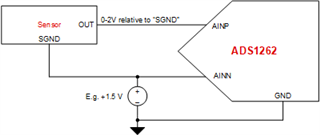
My device will attach to sensors with a standard output of 2V.  I plan to set FSR to 2.5 and would like to bias the voltage using AINCOM = 0.25V to allow room for noise below 0V and above 2V.  Can I do this rather than setting AINCOM to midrange?

Because S and R are often identical, using the PGA will usually put the output voltage above FSR. However there may be portions of the signal where S/R is small and use of the PGA would be useful in reducing noise,  Worst case would be PGA =32, resulting in a 64V input for S/R = 1.0.  Could this damage the ADS1262?

Thanks for your help. 

  • Hi Patrick,

    In principle, the configuration you are describing is commonly-used in a variety of applications. Just make sure to respect the absolute and differential input voltage range limitations on both the VREF and PGA inputs.

    I am not sure I follow what you want to do in the second paragraph. Is the 2V sensor output referenced to ground? And you want VREF = 2.5V, where you are measuring the sensor signal against AINCOM = 0.25V? If so, when the input signal is 0V, you will measure a differential voltage of -0.25V. When the sensor signal is 2V, you will measure a differential voltage of 1.75 V. Also note that the ADS1261 cannot measure ground-reference input signals with the PGA enabled. See Equation 12 in the ADC datasheet for more information.

    The PGA output voltage will be clamped by the supply rails. So as long as the input to the ADC pins is within the recommended operating conditions, the PGA will be okay even if you select a larger gain. However, it may take some time for the PGA to recover from an overload condition. This is not specified in the datasheet, and is just a general observation. The ADS1262 monitors can identify when the PGA output voltage has dropped below the given threshold. Refer to Section 9.3.7 in the ADC datasheet for more information.

    -Bryan

  • Thanks Bryan.  Sorry for the confusion in paragraph 2.  What I want to do is map my 0-2V input signals for S and R to 0,25-2,25 on an FSR of 2,5 so that I don't hit the negative rail with negative noise.  If I do that, can I still ratio the two signals before they are biased?  Does the ratio of signal to the reference voltage precede the application of the bias?  

  • Both S and R are differential inputs,

  • Hi Patrick,

    I am a bit unclear on the terminology you are using. A 0-2V input signal is single-ended, assuming the sensor ground (0V) is the same as the ADC i.e. a unipolar supply. If the signal is single-ended, the ADS1262 PGA must be bypassed in order to operate properly, as you cannot input a 0V signal into the ADC with the PGA enabled (again, refer to Equation 12).

    However, you also mention that your signal (S) is differential, which conflicts with the first statement.

    It seems like you need a bias signal to shift the output of the sensor so it matches the ADC input voltage. You suggested using AINCOM = 0.25V, though this would not shift the signal enough. I drew up a quick block diagram showing how you might configure the bias voltage, your sensor, and the ADC inputs given what I believe is going on with your system. In the system below, a 0V sensor output puts 1.5V at both AINP and AINN. A 2V sensor output has AINP = 3.5V and AINN = 1.5V, which puts the input common-mode signal (2.5V) at the ADC mid-supply voltage (also 2.5V, assuming AVDD = 5V). This is the ideal situation.

    Let me know if this answers your questions.

    -Bryan

  • Thanks Bryan.  I need to go back to the datasheet and read more.