This thread has been locked.

If you have a related question, please click the "Ask a related question" button in the top right corner. The newly created question will be automatically linked to this question.

ADS1220: Designing with ADS1220IRVAT

Part Number: ADS1220
Other Parts Discussed in Thread: INA849

Hi Team,
We are using ADS1220IRVAT in one of our projects.
The same is used for analyzing the pressure applied to a strain gauge.

The following is the setup used.

The Vout is connected to the AIN1 pin of the ADC.
The REFP0 pin is connected to a 5V reference voltage.
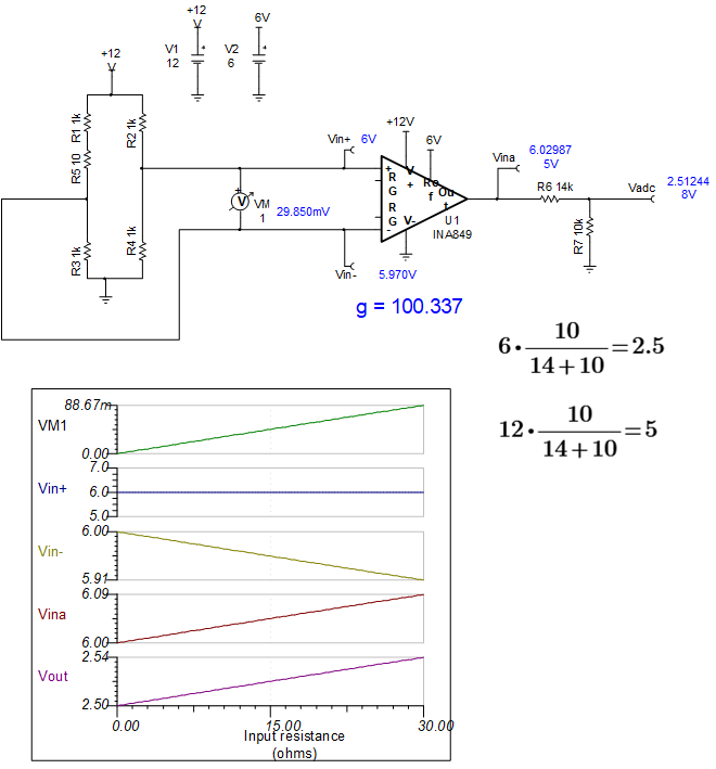
The excitation voltage of the strain gauge is 12V, the opamp is powered from a 12V suply.
Under balanced conditions, the voltage at the input of the ADC is 2.9V and when pressure is applied, the voltage may reach up to 4V.
When we open the circuit of the strain gauge, the voltage will reach up to 7V.
Will it affect the ADC?. I mean a high voltage at the input of the ADC pin.


  • Shibin,

    The absolute maximum rating for the input of the ADC is AVDD + 0.3v (see page 5 in data sheet).  For your application I assume that AVDD =5V, so the maximum input is 5.3V.  Exceeding the absolute maximum will damage the device.  Even though the output of the circuit is 2.9V, the output when the strain gage is open (7V) will damage the device.  If it is possible to reduce the sensor excitation to 5V, this would be ideal.  You can then directly connect the sensor to the ADC inputs and use the ADC PGA to amplifier the sensor output.  If this is not possible I can recommend some amplifier attenuator circuits that will work for your application.

    Art

  • Hi Art Kay,
    Thank you for your reply.
    Yes, the voltage at the  AVDD pin is 5V. 
    I don't think I can lower the excitation voltage of the strain gauge. So connecting the strain gauge directly to the chip will be a suicide mission.
    Could you please recommend to me some amplifier attenuator circuits that will work for my application?.


  • Shibin,

    One simple approach is to use an instrumentation amplifier (INA) to convert the bridge output from a differential signal to a single ended signal.  The output of the INA is then divided by a voltage divider and connected to the ADC input.  One way to use the INA is to set the gain to 1 and the offset so that the output of the INA is near 2.5V.  2.5V is the best common mode input for the ADS1220 when it has a 5V supply.  The voltage divider at the output of the INA will keep the ADC input in a safe range even if the INA output rails.  The ADS1220 PGA can then be used to gain up the INA / bridge output.  The divider in the example circuit below takes the INA full scale output of 12V and translates it to 5V.  The INA offset is set to 6V so that the divider reduces it to 2.5V which is the ADS1220's optimal common mode input.  The INA uses a 12V supply which optimizes the common mode input of the INA to 6V (i.e. it matches the bridge common mode range).  If you need additional gain, then we will need to understand your bridge characteristics better.  You could use a DIP Adaptor EVM to test the INA with the ADS1220EVM.  There are many different INA that will work for this application.  I suggest the INA849 as it has low noise and good offset, but any INA with a supply range greater than 12V should work.  Some things to consider are noise, offset voltage and offset drift.  I hope this helps.

    Art

  • Hi Art Kay,
    Thank you for your reply.
    In our case,
    The bridge resistance is 350 Ohms.
    The excitation voltage is 12V.
    When the bridge is balanced (no load), the output voltage at each output is 6V with respect to the ground.
    The output voltage is 2mV/V, ie, 24mV for 12V.
    If my understanding is correct, if the gain f the INA is set to 1, then the output voltage will be 5.976V to 6.024V as the Vref is 6V.
    1). Is my calculation correct?.
    2). The common-mode voltage of the bridge is nearly 6V, how to calculate the common-mode input of the INA? (is it half of the VCC of the INA?).
    3). What will happen if the common-mode input of INS is not matching with the common-mode voltage of the bridge?.
    4). If a simple voltage divider can be used to scale the output of the bridge to the input voltage range of ADC, why not I can use the same in the first place?. and use the PGA of the ADC. Will it cause any loading issues to the bridge?.
    5). What will be the output of the INA if the bridge is not connected?. ie, the inputs of the INA are floating.
    6). I believe I need additional gain at the output of the INA but in the input voltage range of ADC, like the 5.976V to 6.024V can be mapped to 0 - 5V. Is such a configuration possible?.


  • Shibin,

    1. The easiest and best approach is to set the bridge excitation to 5V an directly drive the input of the ADC.  Bridge sensors are often characterized and specified at a particular excitation voltage, but should work at lower voltages.  The exception to this is when the bridge includes active devices (e.g. an amplifier).  If your bridge is just a resistive bridge I would strongly suggest that you investigate if you could use a 5V excitation voltage.  If you can, you will just use the internal PGA to amplify the differential bridge output. 

    2.  Regarding the INA, You need to consider the difference between common mode voltage and differential voltage.  The 6V output of the bridge is a common mode signal.  If both of the outputs of the bridge are at 6V then the differential voltage is 0V.  The INA will reject the common mode 6V and amplify the differential signal.

    3.  You are correct that the bridge output will be a differential 24mV with a 12V excitation.  Also, for A 12V excitation the common mode output is 6V.  The differential signal will be amplified by the INA and the common mode signal will be rejected.  If the reference pin is set to 6V then the output of the INA will range from 6V to 6.024V. The divider will then translate this to 2.5V to 2.51V.  You can configure the ADS1220 to accept a differential voltage and apply the INA output to the positive input and a fixed 2.5V to the negative input.  This will reject the 2.5V common mode from the INA and the differential will be 10mV.  You can then use the ADS1220 internal PGA to amplify the differential signal.  One problem with this approach is that all the different components will have some tolerance so the 2.5V output from the INA and the 2.5V reference in the negative input will have errors and will not cancel exactly.  Thus there will be an offset introduced by this difference which will limit the gain range.

    4.  Alternatively, you can use gain in the INA.  If the sensor outputs 0V differential when it is balanced (i.e. no stimulus), and 24mV under full load than you can choose a gain and offset to output a single  ended signal that the ADS1220 can use.  For example, you can use a gain of 300 and an offset of 1V for the INA.  This will make the INA output range from 1V to 8.23V.  The output of the voltage divider is then 0.417V to 3.429V.  This signal could be applied to a single ended ADC input.  Keep in mind that bridge sensors typically have offset and gain error so the balanced output will not be exactly zero and the full scale output will not be exactly 24mV.  Thus you need to leave range below zero and above the full scale to account for the gain and offset errors.  That is why the output is scaled from 0.417V to 3.429V instead of 0V to 5V.  You may want to add more margin if your sensor has large gain and offset error specification.  Attached is a TINA spice file that shows this circuit.  This circuit will require that you generate a 1V offset (see voltage divider and op amp in schematic below).  Again, keep in mind that all this extra complexity can be eliminated if you use the bridge with a 5V supply.  Below are pictures of the balanced output and the full scale output.

    5. Please see this document on Bridges.  It is very detailed and may be helpful to you:  A guide to bridge measurements

  • Here is the TINA file.  Note: the switch is used to short the unbalanced resistor.  So when the switch is closed the bridge output is 0mV, when it is open it is 24mV.

    ina and ads1220.TSC

  • Hello Art Kay,
    Thank you for your details answer