This thread has been locked.

If you have a related question, please click the "Ask a related question" button in the top right corner. The newly created question will be automatically linked to this question.

ADS1115: Input protection for negative voltage from saturated opamp.

Part Number: ADS1115

Hi,

I am using an ADC ADS1115 and I am using an high input impedance precision opamp as a voltage follower as opamp buffer before the ADC. The purpose of this setup is to measure feeble voltage of an electrochemical cell. Connecting to ADC directly will load the electrochemical cell so I am using opamp buffer. Electrochemical cell voltage may vary from -200mV to +200mV. As per datasheet ADS1115 can sustain -300mV at an input pin and can measure it using 2s complement method with MSB as 1 for negative voltages. 

8 pin Opamp has standard pinout 

I have applied +-5 V dual rail supply at Vdd and Vss of opamp. The output pin 6 is connected to inverted input pin 2. And pin 3 is signal input. So everything is same as an opamp voltage follower should be. 

When I power up the circuit , the output voltage swings to +ve rail and in my other samples of the precision opamp, it swings to negative rail when no input is connected to pin 3 and it is left floating.

However when I connect actual voltage input to pin 3 then it works fine and precise and follows the voltage properly and neatly.

My concern is why does output swings to either +ve or -ve rail with pin 3 left floating ? The negative swing of -5V may have damaged my ADS1115 perhaps.

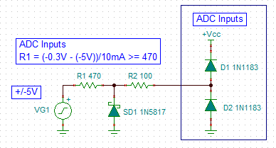
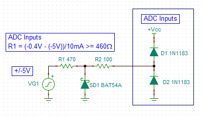
My main issue is to interface the output to an ADC to measure both +ve and -ve voltage output but I cannot stress the input pin of ADC to -0.3 to Vdd+0.3V. I have already damaged one ADC module with this. Please suggest if Opamp is working ok and if I need ADC input protection. And if I need ADC protection then please recommend proper design for ADS1115 input protection with current limit resistor values.

  • Hello, 

    The startup behavior of op-amps can be unpredictable and most op-amps that weren't specifically designed to avoid it, will display a condition where the output saturates to the power-rails during start-up.  The polarity of the glitch to the positive, or negative rail, is dependent on the internal biasing delays of the op-amp input and output stages along with parameters that vary like the supply current and input offset voltage. 

    Best solution would be to add an external Schottky clamp that will limit the voltage at the pin of the ADC to voltages > ~0.4-0.5V.  This diode path will conduct the majority of the energy away from the inputs of the ADC and the current during the negative-overvoltage will be equal to the voltage difference between the overvoltage level and the forward voltage of the diode.  An example is shown below where the Schottky diode current is limited to 10mA with a 470Ohm resistor.  

    If an external clamp can't be added and the internal diodes are forced to conduct, then current must be limited through them similarly to levels less than their abs max ratings of 10mA.  The product was not characterized under these over-voltage conditions and as the datasheet mentions the long-term reliability of the device may be impacted if operating this way.  Therefore, we usually recommend keeping this current <1mA if the over-voltage event will occur regularly over the lifetime of the product.  

  • Instead of 1N5817 diode I am using BAT54S schottky diode set. I hope the resistor values remain same as suggested by you for the job to be done. Please also let me know requirement of 100 ohm resistor R2. Is it to limit current due to forward voltage of 1N5817 Vf divided by R2 ? Like 0.4V/100ohms ?

  • BAT54S is a good diode choice. Replace the datasheet forward voltage into the equation above for the "-0.3V" value that was used for the resistor calculation. 

    You're correct about the R2 resistor.  It's to help limit the current for the remaining voltage difference between the external diode and the internal diodes as they may still conduct a little. If the node the diode is shown at is clamped to -0.5V, you could use the worst-case abs-max value of -0.3V for the internal diodes and limit the current by (-0.5V - (-0.3V)/ 1mA = 200Ohms.  

  • Vf of BAT54S is 0.24V at 0.1mA forward current (If). For 10mA it is 0.4V . How do we redraw the above schematic ?

  • Hello,

    Using the 10mA 0.4V rating for BAT54 here' what you'd have.  If you use the lower 0.1mA Vf values and limit the current, the series resistance is going to start to get high enough that it's going to impact the gain error of the design.