This thread has been locked.

If you have a related question, please click the "Ask a related question" button in the top right corner. The newly created question will be automatically linked to this question.

ADS1262: unwanted level shift at floating signal measurement

Part Number: ADS1262
Other Parts Discussed in Thread: ADS1263

I need to read some radiometric sensors working at UV wavelengths for irradiance measurement.
Each sensor is realized with a photodiode short-circuited to a resistor of 1 kOhm, the photocurrent generated by the photodiode struck by the light is converted into a difference in potential wich can be measured across the resistor; the sensors have a sensitivity of about 0.5 uV / uW cm^-2 and, in my application, they should produce a signal between 0 and 20 mV.

I decided to use an ADS1262 for several reasons, one of them is the presence of a large number of analog inputs and the high sensitivity so I started to test the converter with just one sensor using an Arduino for register settings and readout retrieval.
In this basic test I'm working without amplification at a slow sample rate (10 sps), using an analog supply of 0 to 5 V DC and the internal reference of 2.5 V.
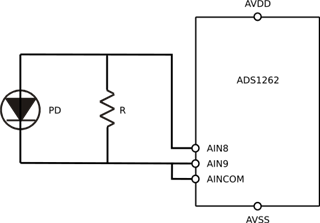
Having to measure an unipolar floating signal I used the internal IC capability to level shift the signal to the half of the ADC input dinamic enabling the VBIAS on the AINCOM pin, as descrbed in the ADS126X datasheet. The schematic of my setup is reported below.

Now the problem: I get a reading with a positive voltage shift of about 20 mV. The shift is present also covering the sensor optical window and doesn't depend on the ADC because if I short-circuit AIN8 to AIN9 I get teh corrent reading of 0 V (except some uV of noise); I've also performed the offset and system calibration. Reading the sensor with a Fluke multimeter measuring mV I get more or less the same readings without the 20 mV shift.

I can't understand from where this shift come out. From what I read on the datasheet the input impedance of analog inputs is high enough (several MOhms) to make negligible the polarization of the sensor resistor caused by the internal VBIAS.

Does someone can help me?

  • Hi Filippo,

    How are you measuring the 20mV offset? This is being determined from the ADC output code?

    And you say that this offset is always there, even when there is not output voltage from the sensor?

    Then, when you short the ADC inputs together (AIN8 and AIN9), the offset goes away - is that correct too?

    I wonder if there is some noise being injected by the AINCOM pin. I am not sure if the VBIAS circuit itself is very low noise. You might try routing the REFOUT pin from the ADS1262 to AIN9 instead of using AINCOM. This should provide a pretty low noise 2.5V source to bias your sensor.

    Let me know if this does not change anything, or if any of my original assumptions are incorrect.

    -Bryan

  • Hi Bryan,

    thank you for your quick reply.

    The answer is yes to all of your questions.

    I've just tried to follow your suggestion, using the REFOUT voltage instead of the VBIAS one, obtaining a slightly lower and more stable offset of about 19 mV, with teh same behavior described in my original post.

    Final test: I replaced the sensor with a 1 kOhm resistor and the offset is still there. Doubling the resistor to 2 kOhm the offset doubles too to about 38 mV. Clearly I'm measuring a voltage drop across the resistor. Supposing the two channel input impedance being the same I get a value of about 130 kOhm.

    I've tried to change the input channels (in different combinations) getting no differences. Also enabling the PGA  the behavior remains the same.

  • Hi Filippo,

    When the PGA is enabled, the input impedance is on the order of GΩ, so it is unlikely that you are seeing input currents or a resistor divider as a result of the PGA impedance.

    Can you send a schematic and the ADC register settings so I can get a better understanding of how your system is physically connected and configured?

    -Bryan

  • Hi,

    here it is the register settings map (I omitted the GPIO ones):

    ID            00000011
    POWER        00010001
    INTERFACE    00000100
    MODE0        01000000
    MODE0        01000000
    MODE1        10000110
    MODE2        00000010
    INPMUX        10001001
    OFCAL0        01001111
    OFCAL1        11111011
    OFCAL2        11111111
    FSCAL0        00000000
    FSCAL1        00000000
    FSCAL2        01000000
    IDACMUX        10111011
    IDACMAG        00000000
    REFMUX        00000000
    TDACP        00000000
    TDACN        00000000

    Doing calculations there is a current of 20 uA flowing through the sensor, I thought it could be a problem with the sensor detection bias but it's disable by default and 20 uA doesn't match any allowed setting. I've noticed that the IC is quite warm, 50 °C more or less, and extracting some heat just by putting a small sink on the surface the unwanted offset drops... I guess something is burned in the analog input stage, even if is difficult to understand what and why.

  • Hi Filippo,

    In your register settings you show MODE1 = 1000 0110. The last three bits (110b) enable a 10Mohm pull-up resistor. This should be disabled for your application. Can you please turn this off and see if things improve?

    -Bryan

  • Hi,

    yes, this configuration was just one of my last try with that device; disconnecting the sensor bias current generator didn't change anything.

    Today I received an ADS1263 (it's really complicated to get them now), replaced to the 1262 on my board and it looks to work fine so I've definitively concluded that the other converter is not working properly.

    I have just another question related to the calibration procedure: working with an input bias voltage like in my case, the system offset and the full scale calibrations have to be performed with or without the bias attached to the negative analog input pin?

  • Hi Filippo,

    When you perform an ADC offset calibration, you short the ADC inputs together and measure the respective output code. This gives you the ADC offset, which can be removed from subsequent measurements. Typically both ADC inputs are shorted to mid-supply (AVDD / 2 = 2.5V for the ADS1263) to keep the absolute input voltage centered in the PGA input range. The level-shift voltage outputs AVDD/2, so this will be a good way to "externally" short the ADC inputs together (enable the level-shift voltage then set MUXP = MUXN = AINCOM). This action will then also calibrate the level-shift voltage to a certain extent.

    The ADS1262 also has an offset calibration command that internally shorts the PGA inputs together, so you could also perform an offset calibration in this manner. But then of course the VBIAS voltage will not be included in the calibration.

    The gain error calibration is typically achieved by applying a close to full-scale input to the ADC. Assuming the gain error is linear, the gain error calibration finds the deviation from the ideal ADC transfer function. This calibrates the gain error of the ADC i.e. not the external system including the sensor. You can refer to section 5.5 in this document for more information about a system calibration: https://www.ti.com/lit/pdf/sbaa532

    This document discusses bridge measurements, but the calibration procedure applies generally to most systems.

    -Bryan