Hello Together,
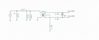
I am using ADS62P25IRGCT in my design, The input clock I am providing is to ADC is by converting single-ended signal to the differential.
The input is from FPGA,1.8V LVCMOS ,125MHz signal. I am configuring the ADC output as LVDS.
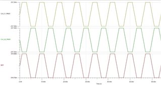
The circuit and simulation result is attached below.
Could you please review and let me know whether the clock side circuit is ok or not
Thanks in advance,
Tensil Sebastian