- Ask a related questionWhat is a related question?A related question is a question created from another question. When the related question is created, it will be automatically linked to the original question.
Hi Team, seeking your assistance.
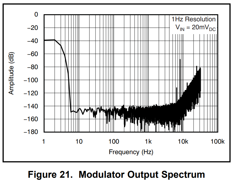
I want to ask a question about ADS1281's digital filter feature. I've read the datasheet, where I learned from the 'Electrical characteristics' that the -3dB cut-off frequency of the FIR filter is 0.413x fdata. But according to Figure 21, it seems that the delta-sigma modulator has a much lower cut-off frequency less than 10Hz. Please tell me how to understand that? Is that means the frequency of my input signal should below 10Hz?
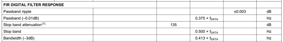
The second question is that I've learned that the digital filter structure is a 5th order Sinc filter followed by an FIR filter. So the '-3dB cut-off frequency of the FIR filter in 'Electrical characteristics' means the overall bandwidth of the Sinc + FIR filter or only means the FIR stage?
Thank you.
-Mark