This thread has been locked.

If you have a related question, please click the "Ask a related question" button in the top right corner. The newly created question will be automatically linked to this question.

LMP92066: Power Supply Sequencing follow-up, concerned about part reliability

Part Number: LMP92066

Hello. During evaluation of this device in my modules I continue to see the negative supply rail run away with excessive current and devices getting damaged, My eval boards have the VIO at 3.3V, VDD at +5V and VSSB at -5V. I have adjusted my test to sequence supplies properly but am still concerned that a turn-on event in my top level assembly can render the LMP92066 part useless because of damage. The damage usually happens if -5V is turned on first, without turning on the +5V or +3.3. This is probably something that should be getting more attention from TI. 

  • Hi Christopher,

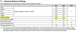
    The condition you describe violates the absolute maximum ratings:

    You are powering on VSSB before VDDB and going beyond the allowed -0.3V between them.

    Best,

    Katlynne Jones

  • Hi Christopher,

    I actually see from your last post that you have VDDB connected to ground. This is definitely violating the absolute maximum ratings for an extended period of time and this could be damaging the DAC.  

    Best,

    Katlynne Jones

  • Hi Christopher, 

    Sorry for the additional reply. I do see that later in the datasheet the device can be operated in 0 to -5V mode and the VDDB can be connected to 0V. The max rating definition makes it seem like this is not allowed. Let me take a closer look.

    Best,

    Katlynne Jones  

  • Hi Christopher,

    Can you give us more details about how you have the FETDRVx pins connected? What PA are you using? Are they connected when you are seeing the damage occur? Are there any other external connections besides the I2C?

    Best,

    Katlynne Jones

  • FETDRV connection go to high impedance GaN gate connections and have the 10nF capacitor as indicated in the datasheet.

     We have our own custom GaN amplifiers that are connected at all times.

     The only thing I am doing differently is connecting the DRVEN pins to “OR” logic gates that are TTL compatible (CAHCT1G32QDBVRQ1)

     If I turn on -5V the negative current increase until I turn on +5V. If I turn on +5V first there is no issue.

     After shutting down the same issue occurs every time, so I can’t leave the -5V on for a long period of time.

  • Hi Christopher,

    I am concerned that you have applied VSS before your system is initialized, and might be causing your gate to have ~0V applied to them.  If you are using GaN PAs, they could be conducting large amounts of current.  Sometimes that also causes the PA to saturate and the gate will actually start sourcing current to the LMP. 

    Could you try removing or disconnecting your PAs to see if that prevents damage? If you cannot, please disable your PA's VDRAIN supply during startup.

    To my knowledge, the LMP92066 itself does not have any specific supply sequencing requirements.

    Thanks,

    Paul

  • Hi Paul, at the point when damage occurs the only supply connected to the module is the -5V. No drain voltage is present. This does not happen on all devices, but when it does there is substantial rework because of the ground paddle on the device

  • I suspect there is some other issue with the schematic or PCB.  Can you monitor the supply voltages (or supply pins) during startup on a typical board? You can leave the ground pad floating for the reworked board as it is only thermally required, not electrically required.  In application you should obviously use the thermal pad, but for these experiments you can leaving it floating to make rework easier.

    Can you share the updated schematic as well?