


Other Parts Discussed in Thread: DAC3162
Hi Team, seeking for assistance.
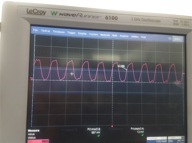
I tried to drive the DAC3162 with an FPGA @ 200MHz. The DAC input is switched from 0x000 to 0xFFF and vice versa at every clock edge to check the full resolution.
I tried to generate the DAC data (DDR format ) as shown in the figure Data transmission format and I send a clock signal 200MHz, Vrms = 0.56V
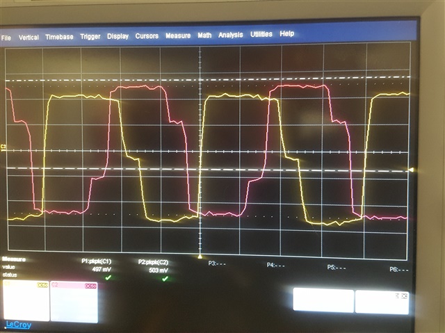
In attached the input clk and the measured outputs signals (you can check also the simulation signals sended to FMC connector of my FPGA)
I need any suggestion to adjust the timing with internal clocking. As infomation, dac is controlled over a fpga. In attached the received clk from DAC3162 and also the two output signals of the dac.
Thank you.
-Mark
