This thread has been locked.

If you have a related question, please click the "Ask a related question" button in the top right corner. The newly created question will be automatically linked to this question.

ADS1220: Extreme noises

Part Number: ADS1220

I am facing noise problems with ADS1220.

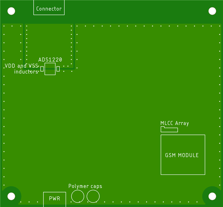
I got placed ADS1220 ADC and a GSM module on the same multi-layer board. When GSM starts transmitting, measurements of ADS1220 starts being inflated.

For reducing amount of problems I am now analysing internal temperature measurements only, but problems are the same for temperature and analog inputs.

Temperature measurements are taken 20 SPS, normal operating mode, continuous conversion, temperature sensor enabled, internal 2.048-V reference, simultaneous 50-Hz and 60-Hz rejection. DRDY pin is checked before reading.

When GSM transmits and antenna is moved by user towards the module (depends on location and surrounding environment), temperature measurements are being increased about 4oC for the entire time of transmission. 

DVDD and AVDD are decoupled with 0.22uF capacitors. DVDD/AVDD and DGND/AVSS are connected through 0.1uH 0805 inductors. CLK connected to DGND and AIN3 is floating. AIN0/1 have anti-aliasing RC filter 47uF - 200Ohm and decoupled from GSM noises with capacitors 10pF/33pF/2.2nF. Power itself is tightly decoupled near to the GSM module and when GSM antenna is placed opposite direction there is no noise, so it is not a general powering problem. If I connect AIN0 and AIN1 pins tight, noises are still present so it is not a noise inducted outside.

It looks that noises are inducted internally inside the ADS1220 (package TSSOP16). What can I do more for reducing the noise?

When I measure the voltage on AVDD-AVSS (every time, not only when GSM transmits) I observe voltage spikes every 2us that are not present on DVDD/DGND. Is it expected?

Example readings (one reading/line per 200ms):

Value converted to oC Value read
23.156250 741
23.156250 741
23.156250 741
23.156250 741
23.156250 741
23.156250 741
23.156250 741
23.187500 742
23.187500 742
23.500000 752
23.156250 741
23.156250 741
23.187500 742
23.187500 742
23.187500 742
23.500000 752
23.968750 767
23.968750 767
25.218750 807
25.375000 812
27.250000 872
27.062500 866
27.250000 872
27.468750 879
27.250000 872
27.281250 873
27.250000 872
27.250000 872
27.062500 866
26.875000 860
23.718750 759
23.625000 756
23.656250 757
23.625000 756
23.718750 759
23.656250 757
23.562500 754
23.500000 752
23.218750 743
23.218750 743
23.218750 743
23.187500 742
23.218750 743
23.187500 742
23.187500 742
23.187500 742

  • Michal,

    There may be many factors in the PCB layout and design that can impact the susceptibility of your ADC system to RFI from the GSM.  I will list some general principles below, but it may be necessary to examine the PCB layout to truly optimize your system.

    1. The first thing I would consider is the usage of the 0.1uH inductor connecting DGND and AVSS. I have seen in many cases that the use of an inductor or ferrite to connect DGND to AGND can cause significant issues.  This is in part because any current that flows between the two planes will generate a transient GND bounce across the inductor.  I recommend that you try replacing the inductor with a zero-ohm resistor. (Attachment Page 1)
    2. It is important that all digital and analog signal traces have a continuous GND plane beneath them. If there is a split or slot in the GND return path beneath the signal trace it creates a discontinuity in the return current.  This can be an issue for emissions as well as susceptibility as this structure acts like an antenna.  (Attachment Page 2 and 3).
    3. The frequency of RF interference applied to low bandwidth devices is normally much greater than the bandwidth of the device. Thus, the RF signal isn’t actually being measured or aliased.  Rather what happens is that the RF signal is rectified by internal diodes and converted to a DC signal.  You might think that the anti-aliasing filter should minimize the RF signal because it’s cutoff frequency is far below the RF frequency range (16.9Hz in your case).  The reason it does not stop the RF signal is that the capacitor has parasitic inductance (ESL) that makes the filter ineffective at high frequencies.  (Attachment page 4).  Some types of capacitors have low ESL, you should check your capacitor data sheet and see if you can find a better high frequency capacitor.  Also, some special X2Y capacitors are designed to act as an EMI filter.  Here is a link to a video showing one of these filters for GSM.  https://www.youtube.com/watch?v=8TWXCVbBTcc
    4. Try to keep all analog signals differential and keep the traces short and symmetrical.
    5. One seldom used approach is to place your GND planes on the outside layer so that they shield the inner layer signal traces. I think in high EMI environments this may be a good idea?
    6. Are you using GND pour on top or bottom layers? If so, you need to make sure that the pour is connected to the internal GND plane with vias at many points.  (see attachment page 5 & 6)

    I hope these tips help you optimize your design.  Below is an attachment that I refer to in the comments.

    Art 

    ads1220 emi tips.pdf

  • Hi Arthur,

    thank you for the detailed and quick reply.

    I replaced the 0.1uH inductor connecting DGND and AVSS with zero-ohm resistor, but testing didn't showed much improvement.

    Designing the PCB I applied most of the EMI guidelines. My inner GND is solid with multiple vias, but (D)GND and AGND are split. DVDD and AVDD are split on the inner layer too. Below I am attaching an example view of my internal power layers (VDD and GND are mostly similar- multiple vias for ICs across the board and without tears). Do you think that for next PCB layout should we apply solid GND, without splitting into (D)GND and AGND (as attachment page 1, right image shows)? Do you think should we apply splitted DVDD/AVDD on the internal layer or make it solid on the inner layer (and actually without any via connection) and make the only connection to AVDD on the top layer? 

  • Michal,

    1. Yes.  I would recommend using a solid GND plane for both AVSS and GND.

    2. I do not think it is necessary to connect AVDD and DVDD into a solid plane.

    3. Thanks for your layout.  Can you provide a little more detail?  How are your analog inputs routed?  Where are the digital signals routed.

    4. What do you mean by "If I connect AIN0 and AIN1 pins tight, noises are still present so it is not a noise inducted outside."  Are you saying that you short the inputs AIN0 and AIN1?

    5.  Can you explain more about the GSM antenna?  How do you adjust the position of the antenna "GSM antenna is placed opposite direction there is no noise"

    6.  RF noise will generally interfere through the analog inputs, reference input, power supplies, GND, digital inputs, or directly into the die.  In your original post you mentioned that you think it may be directly into the die.  Have you considered placing the ADC on the opposite side of the PCB from the GSM?  I don't know if this is practical for your design but the GND plane will act as a shield from the RF noise.

    Best regards,

    Art