This thread has been locked.

If you have a related question, please click the "Ask a related question" button in the top right corner. The newly created question will be automatically linked to this question.

ADS1262: INPMUX register are not saved

Part Number: ADS1262
Other Parts Discussed in Thread: ADS1261, , TIPD188, TPS7A94

Hi all,

Due to the chip shortage, I am not able to source any ADS1261 (let me know if you have a secret stock, I am looking for QTY10).

So I am trying the ADS1262 instead. It is pretty similar but the library I an using is a little different. I am using the lib from TIPD188 example.

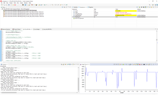
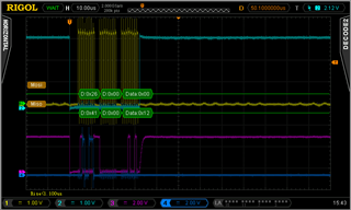
The communication is working well, when I am trying to read to register INTERFACE (0x20+0x02) I receive the 0x05 default value:

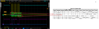
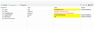
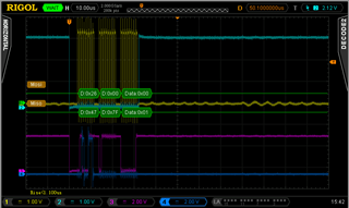
Now I want to configure the pins and references mux to measure my loadcell but I noticed that when I write into the INPMUX register, the value is not saved:

I do a write with MUXP_AIN1(0x10) | MUXN_AIN2(0x02) , then read the register in my while loop:

If I write only one time, instead of reading 0x12 I read the default value 0x01

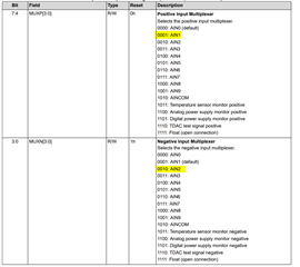
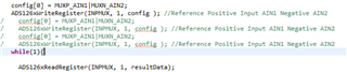
Now if I write twice, I read the right value 0x12:

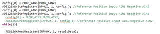
I don't really understand the statement in the datasheet page 87 saying: The MODE2 and INPMUX registers are modified. Typically, register changes take effect immediately after the data are written. However, if the registers are part of a group, then the data are written only after all data for the grouped registers in the write block have been sent.

It means I need to write in all GROUP1 registers to make it saved?

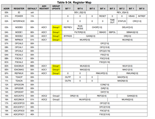
So why writing twice into the register work?

Thank you

  • Hi Hal,

    Just to clarify, the register "groupings" just delay register updates in that group until after you've finished writing to all of the registers in that group when performing multi-register writes. The reason for this is if you were to increase the PGA gain and also switch MUX channels at the same time, you would might otherwise over-range the PGA momentarily if the MODE2 register were to update before the INPMUX register. Instead, these registers are grouped so that writing to both of them in sequence (during a multi-register write command) only takes effect after you finished clocking in the data to both registers. However, if you only write to one register at a time, registers will update immediately after completing the WREG command, as you'd likely expect.

    Therefore, this issue should not have anything to do with the grouping.

    There is a lot of overshoot on the DIN and SCLK signals, between 0.5V and 1V as best as I can tell. Are you able to clean this signals up at all? I am not sure you will get very good results with such noisy inputs.

    You can try enabling the CRC and then reading back the value of the read with the CRC enabled. This can help you determine what is going on based on what you send to the ADC and then what data the ADC provides back.

    Also, does this happen on any other registers? You said that this seems to work okay with the INTERFACE register, though that is just reading back the default value (which is the case when you read back the INPMUX register). Can you test out some other registers before and after writing to them to see what happens?

    -Bryan

  • Hi Bryan, thank you for the support.

    It actually an issue with the SPI on C2000 not the ADS1262. For some reason the first time I write/read on the SPI nothing happen.

    So right now I just do a dummy write/read the first time. Then I can see all the messages that I write and read are OK.

    Now I dig more with the ADS1262 and I experience some spikes in the reading.

    I configured the registers pretty much the same as the example where I set the REF mux to RMUXP_INTP and RMUXP_INTN and then read MUXP_AVDD with MUXN_AVSS:

    //setSTART(1);
        /*********DUMMY READ********/
        ADS126xSendResetCommand(); // dummy stuff to set the SPI
    
        //LoadInitRegSettings();
    
        //ADS126xReadRegister(POWER, 1, resultData);
        /**************************/
    
        //MODE0 (CHOP OFF)
        config[0] = (AdcRegData[MODE0] & DELAY_MASK);
        ADS126xWriteRegister(MODE0, 1, config);
    
        //MODE2 (BYPASS OFF, GAIN = 1 V/V, )
        config[0] = 0x04;//(AdcRegData[MODE2] & DR_MASK);
        ADS126xWriteRegister(MODE2, 1, config);
    
        //Reset OFCAL coefficients
        config[0] = 0x00;
        ADS126xWriteRegister(OFCAL2, 1, config);     //OFCAL2 = 0x00
        config[0] = 0x00;
        ADS126xWriteRegister(OFCAL1, 1, config);     //OFCAL1 = 0x00
        config[0] = 0x00;
        ADS126xWriteRegister(OFCAL0, 1, config);     //OFCAL0 = 0x00
    
        //Reset FSCAL coefficients
        config[0] = 0x40;
        ADS126xWriteRegister(FSCAL2, 1, config);     //FSCAL2 = 0x40
        config[0] = 0x00;
        ADS126xWriteRegister(FSCAL1, 1, config);     //FSCAL1 = 0x00
        config[0] = 0x00;
        ADS126xWriteRegister(FSCAL0, 1, config);     //FSCAL0 = 0x00
    
        //INPMUX (AINP = AIN0, AINN = AIN3)
        config[0] = MUXP_AVDD | MUXN_AVSS;
        ADS126xWriteRegister(INPMUX, 1, config);
    
        //REFMUX
        config[0] = RMUXP_INTP | RMUXN_INTN;
        ADS126xWriteRegister(REFMUX, 1, config);
    
        config[0] = STATUS|CRC_OFF; //0x04
        ADS126xWriteRegister(INTERFACE, 1, config);
    
        while(1){
    
            set_adc_START(1);
            DEVICE_DELAY_US(500);
    //        result = ADS126xReadData(5, 1);
            result = ADS126xReadData(5, 1);
            VoltageReading = (double) result * IntRefVolt / ((double) Gain * exp2(29)); //2^29 to account for 1/4 supply & 1/2 FSR
            SupplyRefVolt = VoltageReading;
            ReadingmV = (int)(SupplyRefVolt*1000);
    
            if ((SupplyRefVolt>6.0))
            {
                GPIO_togglePin(LED_31);  //LED OFF
            }
        }

    I read my AVDD with a DMM and measure 5.125V (+/- 1uV), pretty stable.

    Now if in debug mode I look at the SupplyRefVolt, I have a good result 5.1258V but I also have spikes coming.

    I can see those spikes on the SPI too.

    First question, in my example the datarate is by default 20SPS, what happen when I read the register at 1.6KHz? I should expect to read the same value till a new value is written (every 50ms).

    Second question, the status byte is 0x41 when the data is good and I measure 5.125V. When I see those spike the status byte is garbage:

    Status byte I receive: 0x86, 0x46, 0xA3, 0x14, 0xB1

    I feel like I receive stuff that I should not receive, but during the configuration I made sure I disable CRC and enable status.

    Do you see anything wrong with my config?

    Thank you

  • Hi Hal,

    How do you know when data is ready to be retrieved from the ADC? I don't see any calls to a function that monitors DRDY. Are you retrieving the STATUS byte to know when new data is available instead?

    If you are using read data direct mode, then sending additional SCLKs will continuously retrieve whatever data is in the ADC output shift register. This data should not change between conversion periods, it should only change after each conversion period completes. Therefore if you read data multiple times during the same conversion period, you should be reading the exact same result each time.

    As noted in your scope captures previously, there appeared to be a large amount of noise on your digital signals. I am not sure if this is causing the issue you are seeing, but it is certainly something that should be addressed. I would also suggest looking at the data output using a logic analyzer to better understand what is actually being supplied by the ADC. You mentioned that your previous issue has something to do with the C2000 operation, so it is certainly possible that these new issues are also a result of the processor.

    -Bryan

  • Hi Bryan,

    I added

    while(GPIO_readPin(ADS_DRDY_74)); //wait fopr DRDY to go low

    before reading the data register and now it is good thank you very muchSmiley

    I am confused now, how I was able to read the voltage of AVDD (5V) using the 2.5V internal voltage ref. Normally with a GAIN=1 and ref mux =internal 2.5V, the full scale range is+/-2.5V, but I was able to read my 5.12V supply:

            set_adc_START(0);
            DEVICE_DELAY_US(100);
            config[0] = MUXP_AVDD | MUXN_AVSS;
            ADS126xWriteRegister(INPMUX, 1, config);
            config[0] = RMUXP_INTP | RMUXN_INTN;
            ADS126xWriteRegister(REFMUX, 1, config);
            config[0] = 0x09;//(AdcRegData[MODE2] & DR_MASK);
            ADS126xWriteRegister(MODE2, 1, config);
            set_adc_START(1);
            result4 = ADS126xReadData(5, 1);

    Other than that, I connected my load cell as below:

    Reading AIN1 and AIN2 using the internal ref 2.5V to get a bigger range:

            set_adc_START(0);
            DEVICE_DELAY_US(100);
            config[0] = MUXP_AIN1 | MUXN_AIN2;
            ADS126xWriteRegister(INPMUX, 1, config);
            //config[0] = RMUXP_AIN0 | RMUXN_AIN3;
            config[0] = RMUXP_INTP | RMUXN_INTN;
            ADS126xWriteRegister(REFMUX, 1, config);
            config[0] = 0x59;//(AdcRegData[MODE2] & DR_MASK);
            ADS126xWriteRegister(MODE2, 1, config);
            set_adc_START(1);
            while(GPIO_readPin(ADS_DRDY_74)); //wait fopr DRDY to go low
            result = ADS126xReadData(5, 1);

    The signal is pretty noisy, around (4500000-3500000)=1000000 counts:

    For the full range of the loadcell (compression+tension) I have around 160000000 counts. This gives roughly (4500000-3500000)*100/160000000  = 0.625% noise.

    Changing the Vref from internal to AIN0 and AIN3 gives pretty much the same results:

    around (2200000-1700000)=500000 counts of noise, full range of the loadcell (compression+tension) I have around 80000000 counts, same ration signal / noise.

    So from my understanding, I should keep using the internal Vref , at least I have more resolution. Do you have any thoughts on achieving better reading? I did my best for the layout, followed the design guidelines.

    On my board, the excitation of the load cell is coming from a switching DC/DC 5V that power the rest of the board AVDD=DVDD. The signal is noisy and coupled with the SPI (around 430mV Vp-p), do you think having a low noise LDO 5V will increase the performance I can get?


    I am planning on using a dedicated ultralow noise LDO (LT3045):

    After that I want to connected 3 load cells on the ADS1206. They will have the same excitation and  same reference, do you see any problem with that?
    ADS1262.pdf

    Note that I put a UCC27524DR driver if I want to implement the AC excitation in the future.

    Last question, what is the impact on the choice of clock, Internal oscillator, External clock or External crystal. I could not find in the datasheet what is the rational behind adding an external crystal. What is the gain, better performance?

    Thank you

  • Hi Hal,

    Here are the answers to your questions:

    how I was able to read the voltage of AVDD (5V) using the 2.5V internal voltage ref.

    The supply readback voltage is divided by 4, so it should be ~1.25V at all times. This is why you are able to read the supply voltage using the internal 2.5V VREF, and also why the gain must be 1.

    Do you have any thoughts on achieving better reading?

    See my next answer

    The signal is noisy and coupled with the SPI (around 430mV Vp-p), do you think having a low noise LDO 5V will increase the performance I can get?

    100% yes, please add in a low noise LDO to clean up the switching supply output. Also make sure the switching supply is not located near or crossing over/under the sensitive analog or digital ADC traces, so it cannot couple into these lines and degrade your performance. This is likely what is causing the noise spikes on your SCLK and other digital lines

    I am planning on using a dedicated ultralow noise LDO (LT3045)

    I will also point you to a new family of low-noise LDOs from TI: TPS7A94. These LDOs offer ~50% lower noise compared to LT.

    After that I want to connected 3 load cells on the ADS1206. They will have the same excitation and  same reference, do you see any problem with that?

    Will they be connected in parallel then, where you are measuring the differential output of each bridge with a separate differential ADC analog input? I do not see any issue with this. You can reference our comprehensive bridge measurement guide for more information about measuring multiple load cells: https://www.ti.com/lit/pdf/sbaa532.

    Last question, what is the impact on the choice of clock, Internal oscillator, External clock or External crystal.

    The internal oscillator will be fine for most applications. I would recommend it for bridge measurements for sure. Where you might need an external clock is if you wanted to scale the output data rates to something other than the nominal values, or you wanted to have a higher accuracy clock source. In your case, it probably does not matter, and the internal oscillator will be sufficient. The crystal input is really a legacy option for older systems that often used discrete crystals. I do not see these used very much anymore, and many of our newest ADCs do not offer this as an option. For example, the ADS1261 does not offer a crystal input.

    -Bryan

  • Thank you so much for you help Bryan.

    Will they be connected in parallel then, where you are measuring the differential output of each bridge with a separate differential ADC analog input? I do not see any issue with this.

    Yes they are: 

    I will take a look at the bridge measurement guide and the TPS7A94 for later implementation, but it looks like it is out of stock for now.

  • Hi Hal,

    Thanks for clarifying, this should be good then.

    And yes, many things are out of stock unfortunately. I guess that is what started this thread in fact! So maybe consider the TPS7A94 for a future project then.

    -Bryan