This thread has been locked.

If you have a related question, please click the "Ask a related question" button in the top right corner. The newly created question will be automatically linked to this question.

ADS41B29EVM: ADS41B29EVM

Part Number: ADS41B29EVM
Other Parts Discussed in Thread: ADS41B29,

Hello,

we tried to use the ADS41B29 to convert the received IF signal to digital data. We connected the ADS41B29EVM to the Xilinx FPGA board using the FMC-ADC adapter.  

The ADS41B29 is configured to CMOS interface 2's complement output with the 250MHz input clock. The input signal (IF) frequency varies from 20MHz to 50MHz and different amplitude. The FPGA logic also uses 250MHz to continuously sample the 12bit data.

We found that the data is unstable and noisy time by time. For example, after a high amplitude data, the 10th bit is supposed to be low level, but the bit is kept at high. This problem will also happen in other bits. We have check it by using a oscilloscope. 

Please provide some suggestions / advise to resolve it ? 

Many thanks.

  • Hi KS,

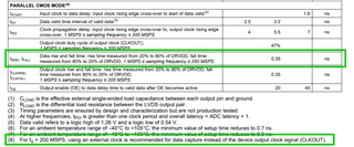
    at 250MSPS, the CMOS interface will have limited rise and fall time due to output and stray capacitance on the PCB lines. This will limit your setup and hold time budget for your FPGA.

    Please see if you can use the same clock that is used for the ADC to capture the CMOS data. The ADS output CMOS clock may have finite slew rate and cause setup/hold time budget limitations.

    Will you also be able to use LVDS interface? This will be the best method for 250MSPS capture. 

  • Hi Kang Hsia,

    I am KS's colleague and thanks for your reply. We did try using the LVDS interface before. However, the FPGA we are using only supports the LVDS25 I/O Standard, which caused the data captured to be much noisier than the CMOS interface.

    Apart from the LVDS problem, I would like to ask for some suggestions about the output buffer. Since the SN74AVC16244DGGR output buffer is not included on the ADS41B29EVM board, how does this buffer affect the CMOS output?

    Many thanks.

  • Hi Yuk Sing,

    Regarding the output buffer, it is recommended to install due to the longer PCB traces and also high speed FMC connector. These connections introduces additional stray capacitance, which is the main reason to reduce your timing budget of setup/hold time. We had to use the buffer in order to capture the data with our TSW1400 EVM.