This thread has been locked.

If you have a related question, please click the "Ask a related question" button in the top right corner. The newly created question will be automatically linked to this question.

ADS131M08: External reference calibration

Part Number: ADS131M08

Hi,

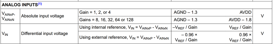
I am using an external reference, and according to the datasheet (Page 7) the VREF is multiplied by 0.96.
Is there any information on how consistent that (0.96) is across different chips and temperature range. Or is it something that I should calibrate for each unit.

Thanks and regards.

  • Hello Afzaal,

    It looks like you've misinterpreted the spec, assuming you're talking about the differential input voltage.

    This is trying to explain input limitations of the differential voltage. With the internal reference, the differential voltage can utilize the entire full scale range, and with the external reference, you could say you have a 4% limitation of that full scale range. For any other readers who need context, we recall the full scale range (FSR) can be represented as FSR = m * Vref / Gain where m = factor that is determined by input type (e.g. true differential, puesdo differential, single ended, etc). More info in this post: https://e2e.ti.com/blogs_/archives/b/precisionhub/posts/it-s-in-the-math-how-to-convert-adc-code-to-a-voltage-part-1 

    The spec is a representation of the losses that result non-linear input behavior when going outside the spec when using an external reference. As a result, I don't think it makes sense to ask about calibration or change over temperature or spec spread. I would recommend thinking of this as a limitation of the inputs that you only get linear behavior for 96% of the FSR when using an external reference. Does that make sense? Instead, this spec usually signals to users if they can handle the dip in dynamic range as a result of using an external reference.  

    Best,

    -Cole

  • Hello Afzaal,

    Actually, I'm getting some clarification from the team so I'll just cross out my answer in the mean time. I should have an answer in the next couple of days.

    Best,

    -Cole

  • Hello Cole,
    Thanks. I'll add a bit to clear up how I read it.

    In case of external reference, the FSR is 96% of VREF. So a VREF of 1.25V gives FSR of 1.2V. Assuming that is correct, my query was how much does the ratio 96% vary from unit to unit and at different temperatures. If it's consistent across units and temperature, then I would only need  to measure my external reference and use 96% of it as FSR, but if it's not then I would need to figure out the ratio too.


  • Hello Afzaal,

    Yes, makes sense. The big question to me is if the 0.96 scaling is in digital or analog. As you could imagine, if its in digital, the 0.96 will not vary with temperature or process. Still talking with the team, hope to have an answer soon.

    Best,

    -Cole

  • Hello Afzaal,

    I've confirmed that the 0.96 adjustment from external reference to reference seen by ADC is in digital so there's no change over temp or process.

    Best,

    -Cole

  • Hello,
    Thanks a lot. I do have one more question.

    Can you also confirm whether the 2/15 ratio for the Internal Test Signal (Page 26) is also digital ?
    Also in case of external reference, whether the test signal is (2/15 * VREF) or (2/15 * 0.96 * VREF).

  • Hello Afzaal,

    I will check with the team on the 2/15 ratio for the internal test signal. 

    As for the test signal, I would change my thinking so that there is a difference between the voltage on the REFIN pin and the VREF voltage used by the modulator (even if its just a digital scale). Since you're using 1.25V at the REFIN pin, the VREF = 1.2V. In other words, it would be 2/15*VREF or 2/15*0.96*REFIN. I get how this is confusing given that VREF is used the differential voltage spec, and I've passed that feedback along to the team.

    Also, 1.2V and VREF is mentioned several times in the datasheet and you should assume they are referring to the VREF voltage, not the REFIN pin voltage. Hope that helps. 

    Best,

    -Cole

  • Hi,

    I asked that because I get different readings when using internal/external references.

    Mean ADC reading of test signal.

    Internal reference : 1068857
    External reference (1.249V): 1125024

    My understanding was that since VREF in both cases is 1.2V, they should be very close, not 5% off. So I (incorrectly) guessed 2/15 was dividing the REFIN. Perhaps something was misconfigured. I'll do a more thorough test soon.

    Thanks.

  • Hello Afzaal,

    Makes sense. And which gain setting are you using for your tests? I'd be curious to know if you're using higher gain settings, and therefore, smaller input voltages.

    Thanks,

    -Cole

  • Hi,
    I double checked everything.
    The clock is 8.3M and the ADC is sampling at 1024 OSR / 4096 SPS.
    Gain is always 0.
    CHx_CFG is initially set to 0x1 to get the offset.
    Which is then written to  CHx_OCAL registers.
    Then CHx_CFG is 0x2 and we calculate the mean of 4096 samples.

    And I still get different readings based on the reference setting.

    I should add that the offsets are also 5% off.

    Internal reference: 1286
    External reference: 1354

  • Hello Afzaal,

    To abstract what I've learned from the team, there's two components to the test signal: the test DAC that supplies it and "feedback" that sets it accordingly. The "feedback" is negligible for temperature and silicon process shift, as it is ratio-metric, for lack of a better term. The test DAC should be not more than +/-1% from the design perspective (for temp and process),

    Is there a practical reason to switch between external and internal in the real system? Or is this a validation exercise?

    Assuming the internal vs. external is output code, I would say its quite a bit off. Your process looks right. Let me go through the same process on an EVM and see if I can reproduce it. Edit: I don't have a clean external reference handy. Using benchtop equipment at hand introduces too much error

    Best,

    -Cole

    Edit: Erased support data claim, the statement from the design team stands.