Other Parts Discussed in Thread: ADS1278
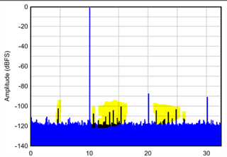
According to a thread, the clock input and SCLK input should have the same clock source to avoid spurs in ADC spectrum (I do not understand what are spurs in ADC spectrum).
I have FPGA connected to the ADC. The clock input to the FPGA is a oscillator of 200MHz. The internal PLL can generate the clock of 13.5MHz, as well as a clock of 27MHz. Can I connect the 13.5MHz to the ADC SCLK pin and the 27MHz clock to the ADC CLK input pin through FPGA IO?The datasheet says a low jitter clock should be used. Is the clock signal through FPGA IO the low jitter IO?
The datasheet says crystal can be used, but I do not know how to connect the crystal to a single clock input pin, In most cases, crystal should be connected to 2 pins of a device.