Hi,
We are setting up a schematic diagram with an ADS7952 (38 pins tssop package) based on SPI communication.
The SPI bus in this design is shared with other slave devices where each slave device can talk back to the
microcontroller as well. This means that in our design all SPI slave devices should be connected with their
SDI signals together, as is the case for all SCLK signals.
However the SSEL output (chip select output) of the microcontroller is connected to a 3-to-8 demultiplexer.
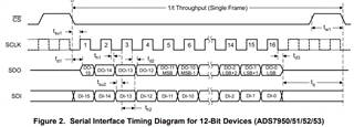
Basically the questions are about the SDO pin :
1) Has the SDO pin of the ADS795x a default (fixed) defined logic level (either "0" or "1") when the chip select
pin = "1" (SPI bus of the chip is deactivated) ?
In a shared SPI bus this means that each SDO pin of an SPI slave device should be connected to some form of
input (or protection) for instance an input multiplexer or tristate buffer.
2) Perhaps in general : should each SDO pin of (all) SPI slave devices of TI be connected with some form of input
(or protection) this way ?
Thx in advance,
Armand