This thread has been locked.

If you have a related question, please click the "Ask a related question" button in the top right corner. The newly created question will be automatically linked to this question.

DAC7574: VOLTAGE MARGINING DAC

Part Number: DAC7574
Other Parts Discussed in Thread: DAC53204

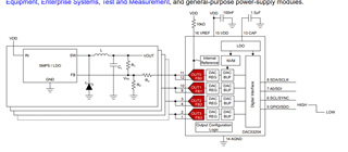
Design in the below image is used in our schematic design , Instead of the Data converter part mentioned in the reference design , we have chosen DAC7574 for our design. Is this part suitable for margining the output of the ldo when the dac output is connected to VFB node through R3 resistor.vdd of our dac is 3.3 and vfb of our ldo is 0.8 . are they any limitations on the value of R3 ?

reference document :Voltage Margining and Scaling Circuit with a Voltage Output Smart DAC .   

  • Hi Dhivya,

    This device can also be used for voltage margining, but you will have to consider the impedance of the DAC during startup and shutdown.  At these times, the output of the DAC will be relatively low impedance to either 0V or an ESD diode forward voltage from 0V.  So your DCDC output might be higher than expected until the DAC is initialized.  The DAC53204 features a high-z output mode at startup to prevent this issue.

    Thanks,

    Paul