This thread has been locked.

If you have a related question, please click the "Ask a related question" button in the top right corner. The newly created question will be automatically linked to this question.

ADS1299EEGFE-PDK: stuck at reading registers

Part Number: ADS1299EEGFE-PDK
Other Parts Discussed in Thread: ADS1299, ADS1298R

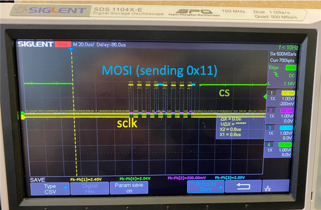
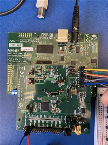
I tried to build interface with ADS1299 through SPI. 

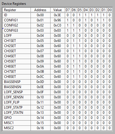
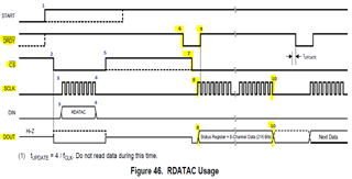
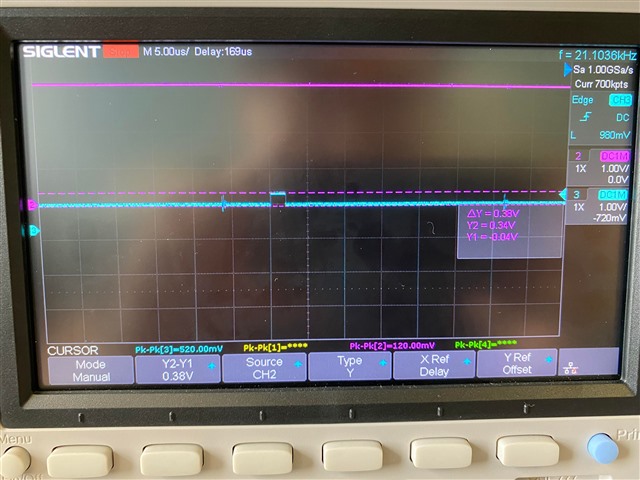
The SPI is not working and the it kept reading 0x00 from ADS1299. 

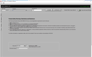
My assumption is that the ADS1299 is not working. So I tried to read the data from the software on PC through UART.

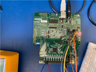
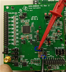
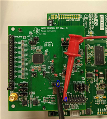
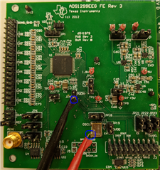
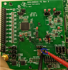
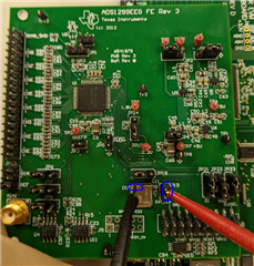
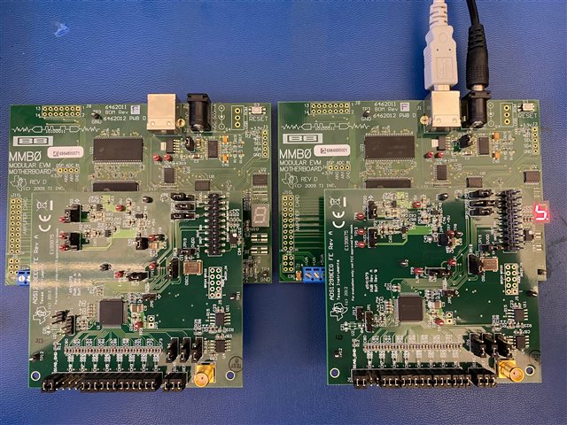
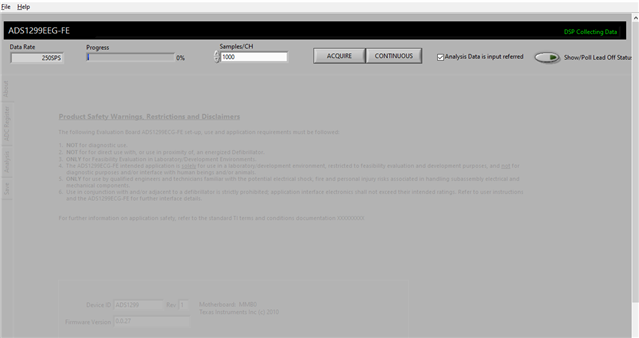
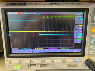
Then it stuck at the reading register step, the data rate is 16000SPS and took over than 15 minutes. After this was done, the software shows no responding whenever I clicked any button on the GUI interface. I found that the seven segment light on MM0 looks like this (picture attached). 

These are what I have tried (MM0 is only connected to PC. The SPI wiring and channel input are all disconnected) :

1. press the reset button on MM0.

2. remove the power jack and connected it again.

3. remove the usb to PC and connected it again.

4. reinstall the software.

5. change the connect PC.

All of above didn't solve the problem. I think this issue is similar to https://e2e.ti.com/support/data-converters-group/data-converters/f/data-converters-forum/412720/ads1298recgf-fe-stuck-at-reading-registers?ADS1298RECGF-FE-stuck-at-reading-registers. But this thread ended up just got a new board. 

Also, I didn't change any hardware setting except that the VDDD is connected to 1.8V.

Could you provide some suggestions on what might cause the issue?

Thanks!

  • Hello Yu-Chi Lin, 

    Welcome to the E2E support forum! 

    On a cursory look, I would recommend you disconnect your own system first and try following the user guide to verify the functionality of the EVM. 

    I'll also have the engineer owning this segment to take a look and provide a response Monday or Tuesday. 

    Kind regards,
    Nick Z

  • Hi Nick,

    Thanks for the update! 

    But as the debugging steps described above, I've already disconnected my own system and the only connection is EVM to PC. Also, I've reinstall the software following the user guide. After power off and then power it on again, the EVM looks fine. But when the software starts to read the registers, the data rate becomes 16000SPS and the seven segment light shows the pattern in the picture. 

    Thanks,
    Yu-Chi

  • Hi Yu-Chi,

      Did you try to use the GUI and EVM with lower Data Rate before connecting to your system? Was it running ok?

      Would you take closer pictures of your MMB0 jumper settings and the ADS1299EVM jumper settings?

      Could you please list what voltages are you supplying to which connector, Jack and port?

      What are the JP2, JP20, JP24 configuration?

       Would you check the following and probe/check the following Test Points' Voltage?

    If you happen to also use an external benchtop power supply, would you please also monitor and note down the current consumptions?

    Thanks

  • Hi ChienChun,

    Thanks for your suggestions!

    It didn't work for slower data rate on GUI before. It had problem reading registers, so it just jumped to maximum 16000SPS data rate and stuck. After double checked the jumper setting. I think the problem comes from the JP24.

    I connected to 1.8V DVDD for my own system SPI interface to EVM.

    But in order to use GUI, it seems that 3.3V DVDD is required. After changing JP24 back to 3.3V, the GUI can now read the register with 250SPS data rate in a minute. EVM is working!

    I have another question. Since I kept reading 0 from EVM (even for read ID command), I used GUI to confirm that the board is working. But the output of my system is 1.8V. To build the SPI interface, in addition to change JP24 to 1.8V, is there other JP configuration that I need to modify?

    Thanks for your help,
    Yu-Chi

  • Hi Yu-Chi,

    Would you try reading values from the following registers or bits using the GUI?

    e.g. Could you read the following using EVM's GUI register map -

    I think by default, it's ADS1299 on the EVM.

    Can you measure the DVDD to DGND,  AVDD to DVDD and /PWDN? 

    If it's possible, would you use scope to check the DIN and DOUT when start reading and make sure the digital signals meet the following limits/requirement -  

    Could you take a look/picture of the JP18, JP 19 and J3– pin 17?

    By the way, the EVM's default OSC1 FXO-HC735-2.048MHZ Oscillator requires DVDD=3.3V to drive the Output and CLK.

    Do you have frequency counter or high sample rate oscilloscope to probe the JP18?

    Thanks.

  • Hi ChienChun,

    This is my Register Map on GUI when DVDD (JP24) is connected to 3.3V. It's ADS1299 on EVM and I think the ID register looks right.
      

    Then, I changed JP24 to 1.8V for SPI to my system.

    I verified all the power supply test points on Table 2 versus TP4 (GND on MM0) and they all matched the table.

    Also, PWDN on J5 is 1.8V relative to TP4. I didn't find on datasheet, but is 1.8V as expected?

    This is the SCLK, CS, and Din(0x11) generated from my system, observed from the oscilloscope, and connected to EVM. I think the digital signal matches the requirements, but the Dout from EVM is always 0.

    I didn't change the setting of JP18, JP19, and J3-PIN17, but this is current setting on EVM.
    JP18: 1-2
    JP19: 1-2
    J3-PIN17: unconnected

    I notice that JP18 is connected 1-2 instead of 2-3, default clock from EVM.

    As you mentioned, the EVM's default OSC1 FXO-HC735-2.048MHZ Oscillator requires DVDD=3.3V to drive the Output and CLK. I am using 1.8V DVDD for SPI. Could I use internal clock from ADS1299? From datasheet, the ADS1299 on-chip oscillator is powered by DVDD, so it should be 1.8V 2.048-MHz clock?

    Also, I am now bit-banging the SPI (clock, cs, Din). In this case, I wonder if the clock of the EVM needs to be at the same frequency of my microprocessor. Would EVM and my microprocessor needs to have the same clock? Or would it be an option to directly connect my system clock to the external clock pin on EVM (J3-PIN17)?

    By the way, I have a 100MHz SDS1104X-E at hand, would it be fast enough to measure the clock signal?
    (Update: I think I should be able to measure through this oscilloscope. I remove the connection on JP18, but didn't get any signal on either 2 or 3 to GND. Neither does 1, since I didn't connect external clock. Is there a way to test the on-chip oscillator clock signal?)

    Also, the seven segment light is on when reading register through GUI, and it's off when reading registers through SPI. I wonder if it should be on.

    Thanks for your help,
    Yu-Chi

  • Hi Yu-Chi,


       I think the EVM and/or EVM's OSC might only support DVDD=3.3V.

       Could you try some more steps to verify this?

       Keep JP19 installed(This supplies DVDD to OSC1 on the EVM)

    1.   Keep JP18 at position 1-2(This uses EXT_CLK coming from MMB0 mother board)

       Supply DVDD = 3.3V and probe JP18 to check the CLK and EXT_CLK signal.

    2. Change JP18 to position 2-3(This uses the OSC1 on EVM as CLK)

        Supply DVDD = 3.3V and probe JP18 to check the CLK and EXT_CLK signal.

    Repeat 1 and 2, but supply DVDD=1.8V.

    To use ADS1299 internal clock,

    Remove/uninstall JP18.

    Install JP23 to position 2-3, this should pull up CLKSEL pin to DVDD Logic High. Please double check.

    You may want to try DVDD=3.3V first and then afterwards, compare it with DVDD = 1.8V.

    Thanks

  • Hi ChienChun,

    First, I would like to double-check. When we say PIN 1, is it from left to right? Or what's the convention of pin numbering in general for the jumpers?

    The test result on EVM is as follow (say the pin right next to JP18 tag is pin3):

    1. when DVDD is 3.3V:
    (1) JP18 at 1-2: has clock signal at 2.05MHz
    (2) JP18 at 2-3: no signal

    2. when DVDD is 1.8V:
    JP18 either at 1-2 or 2-3 has no signal.

    Is there a pin a EVM that I can probe to verify the clock on EVM?
    Also, could you provide the SPI jumper setting or test flow for SPI at VDDD = 1.8V?

    Thanks,
    Yu-Chi

  • Hi,

    The following are common nodes -

    J18-3 and OSC Pin 3 are common; by default, JP18 is in the 2-3 position as shown below; this uses/fetches the Pin 3 of the onboard OSC CLK to ADS1299 CLK pin -

    JP18-1(EXT_CLK) and J3-17(EXT_CLK) are common. Note that usually for through hole components, Pin 1 can be identified/recognized by seeing the soldering pad is Square shape.

    So, if you don't/can't use the on board OSC, which requires 3.3V.  You can install JP18 in 1-2 position, and supply 2.048MHz clock to J3-17(EXT_CLK) from your system.

    The pin 2 of the onboard OSC is identified below and it's common to GND(low side of JP5) -


    The following show that onboard OSC pin1 and pin 4 and DVDD are common if JP19 is installed to supply DVDD to OSC. If onboard OSC needs to be used, the onboard OSC requires DVDD=3.3V and JP19 needs to be installed -

    It seems, if you want to use DVDD=1.8V, you cannot use the onboard OSC(as it requires 3.3V) and need to uninstall JP19.

    You can still try to use ADS1299 internal clock,

    Remove/uninstall JP18.

    Install JP23 to position 2-3, this should pull up CLKSEL pin to DVDD Logic High. Please double check.

    Try with DVDD=3.3V first and then use EVM GUI to toggle/output(i.e. CONFIG1 register CLK_EN bit) the ADS1299 internal CLK to CLK pin -

    You should probe pin 2 of JP18 to check the output CLK. Suggest to get some jumper wires(DuPont or others) so you don't accidently touch/short the CLK pin to the OSC CLK nor the EXT_CLK.

    Then, afterwards, compare it with when DVDD = 1.8V.

    Thanks

  • Hi ChienChun,

    Thanks! I now can get ID between my system and EVM on both DVDD = 1.8V and DVDD = 3.3V. EVM clock only works on 3.3V as you mentioned. Also, for me, in order to use on-chip clock, both JP18 and JP23 need to be uninstalled. Board schematic attached in the end of the EVM datasheet clarified some of my confusions on jumper table.

    But now when I try to retrieve the channel data from EVM. I wonder if DRDY on J3 is DRDY or DRDY bar? After powerup, I saw that pin signal low, jumped to VDD for short period (0->1 pulse), and back to low, on oscilloscope, which is opposite from datasheet.

    Thanks,
    Yu-Chi

  • Hello Yu-Chi,

    Due to the July 4 US holiday, our responses are delayed. 

    Please expect response from Chien by Wednesday July 6 or earliest.

  • Hi Yu-Chi,

    #DRDY or /DRDY or DRDY bar is negative asserted(i.e. active low) as stated in ADS1299 datasheet page 6.

    Page 41 Figure 46. does not represent the power up or initialization sequence, it shows the timing diagram when the ADS1299 is running in Read Data Continuous Mode. i.e. if there will be data ready to come out from the DOUT pin, ADS1299 /DRDY should go low first to indicate/signal the host to pull the /CS to low first and then waiting host to start SCLK to clock/shift the data out from DOUT -

    I roughly number the STATES on the timing diagram, STATEs 6 to 10 indicate what may be happening when acquire data in RDATAC continuous mode -

    Thanks 

  • Hi ChienChun,

    I think I understand how DRDY works. On EVM J3, it's DRDY not DRDY bar. Probably that's why the I saw active high.

    But now I had another issue similar to this one. https://e2e.ti.com/support/data-converters-group/data-converters/f/data-converters-forum/1017085/ads1299-data-ready-pin-not-going-low

    The EVM can get data from Arduino through SPI yesterday. But the next day when I powered it up, it no longer worked. I didn't change software code or any jumper setting. I found that the DRDY pin always stay high. 

    Then I removed the all the SPI connections on EVM and just powered it up again. I compared this EVM to another one. They both have the same default jumper setting as datasheet suggest. But the right one can be read from the software, while the left one stuck at the DSP collecting data. Also, the DRDY pin of the left one still stays high, while the right one has periodic pulse showing that data is ready.

    Could you please provide some suggestions on how to solve this issue?

    Thanks,
    Yu-Chi

  • Hi Yu-Chi,

      DRDY shown on the PCBA silk screen might be the designers mistakes as in the ADS1299 datasheet and EVM user guide page 16 Table 8, it all shows DRDYB bar.

     Can you connect the EVM kit(with default configuration) that is suspecting to have issue to the PC and use GUI to click the RESET button with Programmed Defaults?

     Also, I may suggest you do some critical Test Points(TP) voltage probe and check with user guide Page 15 Table 2, 3 and 4.

    If possible, monitor the REST bar and DRDY bar pin when you click the "RESET" button and "ACQUIRE" button on the GUI. Let's not use the CONTINUOUS button.

    Two important notes for reminder-

    1. If other external system or host is connected to the EVM, please make sure the GND are the same and minimize the ground loop.

    2. logic high and low signals that come from other external system or host need to meet the digital input voltage level requirement e.g. 1.8V or 3.3V depending on the EVM's DVDD settings mentioned in ADS1299 datasheet.

  • Hi ChienChun,

    For ready pin, what I observed is the same as #5 in this link: https://e2e.ti.com/support/data-converters-group/data-converters/f/data-converters-forum/775288/faq-ads129x-how-do-i-verify-that-my-ads129x-device-is-still-functional/2868597#2868597. I am confused.

    I connected the trouble EVM kit to PC and used GUI to click the RESET button with Programmed Defaults. But the problem stays the same. It stuck at DSP collecting DATA with 250SPS data rate without any progress. (It can read register and shows sync complete...Ready when running GUI in the very beginning. But when I click ACQUIRE, it stuck.)

    I've checked all the TP on Table 2, 3, 4 and they are as expected.

    Do you mean RESET bar and DRDY bar pin on J3? What is expected to see on the oscilloscope when click the RESET and ACQUIRE button?

    When I power it up(the only connection to EVM is power jack) and monitor the DRDY pin on J3, the working EVM shows 3.3V pulse as expected, while the other one shows only 300mV. I suspect this is the reason why the GUI stuck and can not read the data. Could you point me out on how to solve this issue?

    BTW, thanks for the remainder! But the above steps are tested without external system connected. Or at least, only oscilloscope.

    Thanks,
    Yu-Chi

  • Hi Yu-Chi,

    Are the DVDD, TP7, TP8, TP9 and TP10 of both EVM the same or different?

    Did you try the same steps, e.g. establish connection with GUI, RESET with Programmed Defaults, ACQUIRE. with the EVM that doesn't have issue? How does it response?

    Can you probe and compare CS bar pin on both EVMs?

    If all above work on the non-issue EVM, but the problematic EVM still doesn't work after several reboot and/or power cycle, I am afraid something might damage on the problematic EVM or the MMB0 mother board associated with the problematic EVM.

    Do you have the MMB0 mother board's schematic? Disconnect/remove the problematic EVM from the MMB0 board, and only supply power to the MMB0 board without connecting to PC. Could you probe/check voltage on MMB0 board at

    J12-pin1 =5V,

    high side of C40 = 1.6V,

    high side of C41 = J3-pin1 = J6-pin1 =J5-pin9 = 3.3V,

    high side of C31 = J5-pin10 = high side of J13A and J13B = 5V,

    high side of C25 = J5-Pin7 = 1.8V

    Thanks

  • Hi ChienChun,

    DVDD, TP7, TP8, TP9 and TP10 of both EVM are the same as the datasheet.

    I tried the same process, "establish connection with GUI, RESET with Programmed Defaults, ACQUIRE", with both. I didn't observe any different after doing these steps. The working one still worked and the problematic still doesn't work.

    I probed the CS bar pin on J3-pin1, and it is 0 volt on both EVM.

    I didn't have MMB0 mother board's schematic and it would be great if I could have access to it. For now I just looked at the label on the board.
    I could find the pins you mentioned and tested, and they are all matched as you listed. (only mother board connected to power jack).

    Also, I am now playing around with the working one SPI. I can read registers and get the same value as GUI. In addition, I can write to the register and read register again to confirm writing. But I was not able to read the data, or the data seems to be junk. Due to system requirement, this is the one that operate at 1.8V DVDD. I had 3.3V working on Arduino system, and what I am doing is change JP24 to 1.8V and replicate the code on my system. Is there anything else that I need to take care of when switching to 1.8V?

    Thanks,
    Yu-Chi

  • MMB0 Mother board schematic -

    MMB0 motherboard 1121.MMB0_Sch_RevD

    MMB0 motherboard 1121.MMB0_Sch_RevD.PDF

    If the DRDY bar signal doesn't behave correctly, it's risky to use and believe the DOUT.

    On the problematic EVM, wondering if you could write the following to configure GPIO1~4 to output high and check/probe the GPIO1~4 on J3 pin6, pin12 and J5 pin8, pin 6 to see if they could output high logic?

    ADS1299 datasheet page 58 -

    GPIO: General-Purpose I/O Register (address = 14h)

    Write GPIOD all 1s(i.e. set all data to be output to 1s) and GPIOC all 0s(i.e. configure all GPIO to outputs), i.e. GPIO register = 1111 0000

    This may help us know whether it's only the DRDY bar has issue.

    Let me take a look for the 1.8V application and get back to you.

    Thanks

  • The problematic EVM DRDY bar doesn't behave correctly and the voltage I probed is the same as you suggested.

    While trying to figure out the problematic EVM one, I am using the working EVM for 1.8V SPI. This one got correct data with 3.3V, but have problem with 1.8V.

    Thanks.

  • Here's the updated test result. I connected the problematic one to GUI and set register 0x14 to be 1111 0000 (0xF0). Then, I probed the J3 pin6, pin12 and J5 pin8 and pin6, they are all 3.3V.

    Please let me know if there is other tests I could do. Thanks!

  • So, it's the DRDY bar pin has issue.  I don't know if you still want to use the problematic one?

    For the good work EVM,

    Do you set DVDD=1.8V?

    Could you probe/check the DVDD with respect to DGND? and AVSS to DGND? by referring to ADS1299 datasheet page 7 section 7.1

    If your DVDD is 1.8V, please make sure all other digital signal/logic are no more than DVDD+0.3V.

    Note: setting DVDD=1.8V on EVM may lead to the EVM not work/support the MMB0 mother board as the TMS320VC5507PGE's DVDD requires & uses 3V3 solid from  MMB0 mother board, so it may not read low voltage digital signals correctly. i.e. with EVM set/configure to DVDD=1.8V, the EVM can only be communicated and relied on your low power/voltage host(Arduino ?)

    The OSC on EVM doesn't work/support DVDD=1.8V for CLK signal.

    To use the ADS1299's built-in internal clock for CLK signal,

    Let's uninstall JP18 and JP19 to prevent any accidental clock conflicts.

    And then, it requires to wire/configure the CLKSEL PIN to high either by driving logic High(with respect to the DVDD selected) or Pull-Up resistor to DVDD by JP23 in ADS1299EVM user guide page 53. Again, with EVM set/configure to DVDD=1.8V, the EVM can only be communicated and relied on your low power/voltage host(Arduino ?)

    You may also try to generate/drive a clean CLK signal to CLK pin from your host.

    Thanks.

  • I'll use the working one for now. But it would be great if I know where the issue comes from. If this happened due to my wrong usage, I hope to prevent it from happening again. (The problematic board was bought mid-April this year)

    About the DVDD = 1.8V, now it can read registers and write registers, such as reading register value, and modifying registers and reading back. So I think the ADS on-chip clock that I am using is working correctly. (I have similar jumper setting as you suggest and I can probe clock on JP18-pin2). But the problem is that I can not read correct data in RDATAC mode. I wonder if this happens due to DRDY pin. The first 24-bit status register I got is 0xC00000, which matches the datasheet. But the remaining channel data looks like junk. With or without signal input, I always get the same repeated junk pattern regardless of channels. Does the SPI_CLK signal need to always toggle even when there is neither read nor write command?

    This is the waveform when reading data in RDATAC mode. (yellow: SCLK, blue: CS bar, green: DRDY bar). This is similar to Figure 46 on p.41 but the only difference is there is a pulse of DRDY. I wonder if this is expected. I am still confused about DRDY (or DRDY bar) behavior.

    Could you point me to some possible mistakes that I make? 

    Thanks!

  • Hi,

     There could be several factors that could cause the problematic EVM's DRDY bar stops working correctly, e.g. ESD, handling, accidently connect to GND or much lower potential without current limiting resistors or the DVDD and the logic signals voltages do not match/comply or imbalanced ground plane/reference.

    By the way, since you are using ADS1299 internal clock(CLK), you have option to send the built-in CLK signal out to CLK pin by writing 1 to "CONFIG1.CLK_EN BIT" as described in page 27, but this is optional.

    How does read the 'ID: ID Control Register (address = 00h)" (ADS1299 datasheet Page 45) work? Can you read the values shown in Table 12?  

    What about just "RDATA: Read Data" described in ADS1299 datasheet page 42? Does it work? what is your SCLK frequency? and Data Rate(DR) setting?

    Did you use/send START command to start or use the START pin? How is the START pin connected?

    Page 34, figure 40 and Table 7 show there is settling time required, tSETTLE(depends on fCLK and DR[2:0] bits)

    Page 35 shows how DRDY bar works -

    Could you also probe&show DIN and DOUT?

    Would you separate the signals in vertical position a bit to better distinguish?

    From Figure 46 or 47, we should see once DRDY bar falls edge, host should pull the CS bar to low and starts sending RDATA command and SCLK at the same time before DRDY bar rises edge.

    Note that on page 12, make sure to wait after CS bar falling edge long enough before sending SCLK depending on the DVDD voltage - tCSSC Delay time, CS low to first SCLK. And, there is tDOPD(Propagation delay time, SCLK rising edge to DOUT valid)

    You may also take a look of this thread that shows the timing diagram for ADS1298R

  • Hi ChienChun,

    For the problematic one, do we conclude that it is broken? Is there a way that I can fix it myself? What is the next step we usually take this situation? Do we send it for repair or replacement?

    Also, thanks for your suggestions. My problem for SPI data comes from some delay in between each sample (RDATAC mode), so that it's not faster enough to capture the all 216bits data. It's somewhat solved, but the first cycle data looks weird. (the input to channel is 2mVp-p sine wave and square wave respectively, and I plot the raw data on Matlab) Do you have clues on what might happen by any chances? Also, I didn't get the link of the timing diagram for ADS1298R. Could you please send me again?

    BTW, on J3, it's DRDY bar as you suggested. Sorry I misunderstood before. When power on, it looks like _|_|_|_|... because data is not being read.

    Thanks,
    Yu-Chi

  • HI Yu-Chi,

    Where did you get/purchase the problematic EVM from? You may try contact the vendor to see if they could send an replacement EVM.

    Here is the timing diagram for ADS1298R, similar but not exactly the same as ADS1299 -

    https://e2e.ti.com/support/data-converters-group/data-converters/f/data-converters-forum/775262/faq-ads129x-i-m-having-trouble-communicating-with-my-ads129x-device-via-spi-what-debug-steps-i-should-try/2868427#2868427

    "the first cycle data looks weird. (the input to channel is 2mVp-p sine wave and square wave respectively, and I plot the raw data on Matlab) Do you have clues on what might happen by any chances? Also, I didn't get the link of the timing diagram for ADS1298R. Could you please send me again?"

    What was the test signal source you used to generate those waves? Was it external?

    Had the source already output test signal before you started acquiring? Did you follow the proper power up sequence and do a "RESET" and wait a bit before some of your initialization routine, and wait a bit before start acquiring? You may refer to ADS1299 page 70 Power-up Sequencing -

    Do you want to try use the internal test signals source as described in ADS1299 page 47 CONFIG2: Configuration Register 2 (address = 02h)?

    Thanks.

  • Hi ChienChun,

    Yes, the signal was external 2mVp-p square wave and sine wave respectively. I now can get signal data from EVM through SPI. I think my problem came from the Vref, which is default to external voltage on EVM but on EVM that pin is open. After modifying the Vref to internal reference voltage, waveform looks as expected. 

    Thank you so much for your help along the way,
    Yu-Chi