This thread has been locked.

If you have a related question, please click the "Ask a related question" button in the top right corner. The newly created question will be automatically linked to this question.

ADS131E08: Error reading ID through SPI

Part Number: ADS131E08

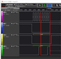
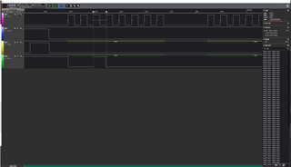
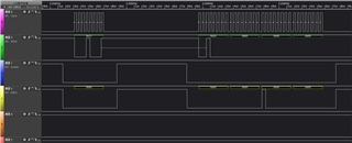
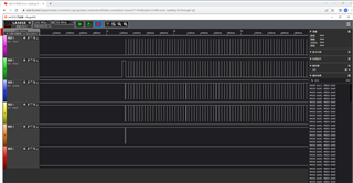
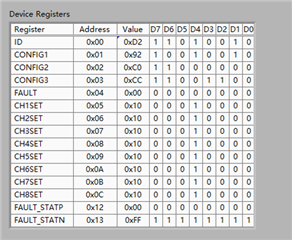
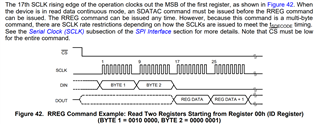
According to the instructions of the datasheet, I send the SDATAC instruction first, then delay 2μs (frequency is 2MHz), then send 0x20 0x01 (ID register address is 00h), resulting in the following waveform.

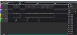
It seems that after I send the data, ADS131E08 does not have any response, I would like to ask what might be the problem?

  • Hello Zhen,

    Thank you for your post.

    In the image below, MOSI is changing on the SCLK trailing edge and the SCLK leading edge is used to capture data. Instead, you need to use the SCLK trailing edge for data capture because this is what the ADC interface is expecting. Please change the SCLK settings in your microcontroller to SPI Mode 1 (CPOL = 0, CPHA = 1).

    Regards,

    Ryan

  • Thank you for your reply.

    After I changed the phase, I still couldn't get the ID number.

    You know what else might be a problem?

  • Hello Zhen,

    There are two other important timing specs to verify. First, please check the tCSH timing. This is the required time for CSn to remain high between consecutive frames (= 2*tCLK).

    Second, please check the tSDECODE time for multi-byte commands (i.e. RREG). This is the time required between the end of the first byte and the end of the second byte. What is your SCLK frequency? 

    Regards,

    Ryan

  • In my Settings, CLK=2.048MHz, SCLK=2MHz, tCSH minimum 2tCLK.

    The measured tCSH is 58.45296ms, which should meet the requirements.

    In addition, tSDECODE is 5.54us, which meets the minimum requirement of 4tCLK.

  • In addition, I found that during transmission, the frequency of one cycle in the middle (A1-A2) suddenly became smaller, from 2MHz to 1.92mhz. Will this have any impact?

  • Hello Zhen,

    Thanks for verifying the timing specs. I agree the tSDECODE spec looks correct. However, the tCSH is the time from CSn rising edge to the next CSn falling edge. In your original post, it appears to be about 3.5 us (which is long enough).

    After sending the two-byte command (0x20 0x01), you must send two more null bytes (0x00 0x00) in order to read out the register data. Your original post showed the correct byte sequence, but the last post only sends the RREG command.

    Do you see DRDYn toggling after start-up? This would help confirm the device is powered up correctly. If not, can you try issuing a RESETn pulse on the device pin after the supplies have fully ramped?

    The measured SCLK period in your last image is likely just the limitation from your logic analyzer capture bandwidth. As a result, you may notice some occasional inaccuracies that do not represent the true SCLK period and duty cycle.

    Regards,

    Ryan

  • Thanks you for your reply. I tried your first suggestion, but still didn't return the correct ID.

    According to this paragraph, I offered +5V(AVDD) and 1.8V(DVDD).

    In addition, in power-supply Test Points, except TP10 is 0V, the voltage of other Test Points is correct.

    So I think the power supply should be normal. As for DRDY, I downloaded the program to DSP about a minute after I powered it on and observed that it was always at high level.

  • Hello Zhen,

    I did not realize you were using our ADS131E08EVM-PDK. Are you using the MMB0 board or connecting an external controller to the daughterboard? If you are using your own controller, my recommendation would be to disconnect the MMB0 and provide the external power supplies directly to the test points or jumper pins. Remember to connect your external power supply ground to the EVM ground using the available test points. 

    For DVDD = 1.8 V, connect a 1.8-V external supply to TP9 and configure the JP11 jumper to the [1-2] position.

    For AVDD = 5.0 V, connect a 5-V external supply directly to JP1[2] (do not install a jumper). Also, configure JP7 jumper to the [1-2] position (AVSS = AGND).

    The power supplies above are what is required to use the SPI interface. In order to begin ADC conversions, there must be an active clock (internal or external). To choose the internal 2.048-MHz clock, uninstall the jumper on JP10 so that CLKSEL = 1. To use an external clock source, install the jumper on JP10 in the [1-2] position (CLKSEL = 0). You can use OSC1 as the external clock (JP6[1-2] and JP5[2-3]), or you can provide an external clock directly to JP5[2] (configure JP6[2-3] to disable OSC1). Assuming the START pin is high and clock is active, you will see DRDYn toggle after start-up at the default data rate.

    Regards,

    Ryan

  • Hello Ryan,

    I think I may have found the problem.

    First, I want to confirm that if YOU want to use OSC1, according to the circuit diagram, it should be connected to JP5[1-2].

    Then, I connected JP10[1-2], JP5[1-2], JP6[1-2]. Also, I connected JP5[1] to the logic analyzer and found no waveform (channel 5 connected to JP5[1]).

    So, I wonder if there's something wrong with the Active Clock.

  • In addition, I read such a passage from the ADS131E08EVM Datasheet. When I use 1.8V DVDD, the oscillator is Sit8002AC-34-18E-2.048, but I can't find this oscillator in the circuit diagram, only SEE FX0-HC735-2.048.

  • Hello Zhen,

    The pin labels you drew in your schematic are incorrect. Pin 1 of the jumpers is indicated by the notches in the jumper schematic symbol. Please recheck your jumper settings.

    OSC1 can be replaced with Sit8002AC-34-18E-2.048 device for 1.8-V DVDD operation. I did not realize the default device only works with 3.3 V. For your setup, is an external clock required? If you can use the internal clock, this would be simpler for your evaluation. For internal clock:

    1. remove the jumper from JP5, 
    2. install JP6[2-3]
    3. remove the jumper from JP10

    Regards,

    Ryan

  • Thanks again for your reply.

    I would also like to use the internal clock, but I see that the datasheet is Not installed, which means EVM does Not provide an internal clock?

  • "Not installed" refers to the jumper on JP5 (same as step #1 in my previous reply).

    Regards,

    Ryan

  • I'm sorry that I didn't have time to read your reply for something I did a few days ago.

    I configured the internal clock according to the steps you gave, and I got no response.

    However, when I give the board 3.3V and set CLKSEL Pin=0, select OSC1, then I can get the internal clock.

    There are three clock modes (internal, 1.8V, 3.3V). I can only get 3.3V internal clock.

  • I know why the internal clock isn't working.

    Based on THE ADS131E08 Datasheet, if I want to use Internal oscillator, NOT only do I need to set CLKSEL_PIN to 1, but I also need to set CLK_EN BIT to 1.

    However, I found that the CLK_EN BIT is 0 by default, and the result of the image below is what I got from adS131E08EVM-PDK-sw.

    As a result, the board is currently only able to generate internal clocks using OSC1 by using 3.3V (since I can't modify CONFIG1)

  • Hello Zhen,

    Based on THE ADS131E08 Datasheet, if I want to use Internal oscillator, NOT only do I need to set CLKSEL_PIN to 1, but I also need to set CLK_EN BIT to 1.

    This statement is incorrect. The internal oscillator is active whenever CLKSEL pin is high. By default, this internal clock signal is separated from the CLK pin itself (CLK_EN = 0b). However, if you wish to probe this signal or connect it to another circuit, then you can set CLK_EN = 1b and the internal oscillator will be driven to the CLK pin as an output.

    Once the internal oscillator is selected and the START pin is high, you will see the DRDYn pin toggling. This is another way to confirm the device has started properly.

    Regards,

    Ryan

  • Hello Ryan,

    I found that the only way to use EVM as a stand-alone board was to use 3.3V FX0-HC735.

    When I combine EVM with MMB0, through ADS131E08 Evaluation Software, I can configure CONFIG1 so that CLK_EN=1 and successfully get the internal clock signal.

    However, once I separated EVM from MMB0 and tested it again, I found CONFIG1 reset and CLK_EN=0.