This thread has been locked.

If you have a related question, please click the "Ask a related question" button in the top right corner. The newly created question will be automatically linked to this question.

ADS8661: How to read digital voltage by using ADS8661 (Raspberry Pi platform)

Part Number: ADS8661
Other Parts Discussed in Thread: ADS8861,

Hi Team,

I want to check the procedure of reading voltage by using ADS8861. Would you help check below procedure for us? Thank you.

Platfrom : Raspberry Pi,  SPI speed, = 15.25878906kHz

SPI interface, SDO-O, SCLK, CONVST/CS, SDI

REFIO , REFCAP, connect to cap

DGND, AGND, REFGND, AIN_GND to GND (Raspberry Pi board GND)

AVDD = 5V, DVDD = 3V (Raspberry Pi supply the power)

Program procedure :

RST : high -> delay 1 ms -> low -> delay 1 ms -> high


Register parameters writing :                                             

DEVICE_ID_REG(0x02)              -> data (0x00  ,  0x0c)   (address 0x03 下0x00 data, address 0x02 下0x0c data, )      

RST_PWRCTL_REG (0x04)       -> data (0x69  ,  0x03)

SDI_CTL_REG (0x08)                -> data (0x00  ,  0x03)

SDO_CTL_REG (0x0C)              -> data (0x00  ,  0x00)

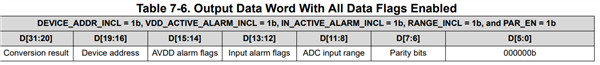
DATAOUT_CTL_REG (0x0C)    -> data (0x55  ,  0x08)   -> output data word with all Data Flags Enabled

RANGE_SEL_CTL_REG (0x0C) -> data (0x00  ,  0x0B)   -> internal reference 4.096V , Range = 1.25 *4.096 = 0 ~ 5.12 V


We want to read digital voltage via ADS8861. ( We placed an voltage input on AIN_P.)

Now we can detect the Raspberry Pi Device_ID. 

I want to know how to explain the data we read.


Below is our measurement result.

0x00b10c00  (GND)

0x00b13c5c  (1.834V)

0x00b23c2d  (3.443V)

0x00b27c6d  (4.82V)

Regards,

Roy

  • Hello Roy,

    The pin image you shared does not correspond to the ADS8861, would you confirm the device part number?

    Regards

    Cynthia

  • Hi Cynthia,

    Excuse me. It should be ADS8661.


    Roy

  • Hi Roy,

    Please see my feedback and questions below:

    1. RST_PWRCTL_REG (0x04):  you set PWRDN to 1 which puts the converter into power-down mode. Is this expected by you?
    2. SDI_CTL_REG (0x08): you set SDO to 11b mode. What's your SPI configuration on your microcontroller?
    3. SDO_CTL_REG (0x0C):  this command does not do anything because the reset value for this register is already all 0s.
    4. DATAOUT_CTL_REG (0x10?): register value, ACTIVE_VDD_H_FLAG, ACTIVE_IN_H_FLAG, Input range and two parity bits are included in the output bit stream.

    These code seem incorrect, please let me know the answers for my questions. I have more questions, what's your sampling rate? What's the voltage measured on the REFIO and REFCAP pin? Did you read back each register to make sure whether your register writing are correct or not?

    Also, Can you please share your timing for register writing? and a timing for data conversion? the timing should be captured with an oscilloscope for SCLK,/CS, SDI and SDO.

    Thanks&regards,

    Dale

  • Hi Dale,

    1.    RST_PWRCTL_REG (0x04):  you set PWRDN to 1 which puts the converter into power-down mode. Is this expected by you?   [Roy] We removed it.
    1. SDI_CTL_REG (0x08): you set SDO to 11b mode. What's your SPI configuration on your microcontroller? [Roy] Raspberry Pi has set SPI_MODE00 , and so we have set ADS8861 = 00b
    2. SDO_CTL_REG (0x0C):  this command does not do anything because the reset value for this register is already all 0s. [Roy] ok.
    3. DATAOUT_CTL_REG (0x10?): register value, ACTIVE_VDD_H_FLAG, ACTIVE_IN_H_FLAG, Input range and two parity bits are included in the output bit stream. [Roy] Excuse me, it typo, DATAOUT_CTL_REG (0x10) ,  RANGE_SEL_CTL_REG (0x14)

    These code seem incorrect, please let me know the answers for my questions. I have more questions, what's your sampling rate? What's the voltage measured on the REFIO and REFCAP pin? Did you read back each register to make sure whether your register writing are correct or not?   

    [Roy] We used two way devices with wrong SP_MODE to read the register was the same as the content that we wrote.

    Also, Can you please share your timing for register writing? and a timing for data conversion? the timing should be captured with an oscilloscope for SCLK,/CS, SDI and SDO.        


    Now we fixed some issues, but still has some questions needing your comments,

     After modification, we can read digital voltage. (0~5.12V -> 0x000~0xfff)


    1st byte that Raspberry Pi read is ADS8861 MSB, CPU read value should be opposite, and so we transformed it. Now setting is showing as below.

    DEVICE_ID_REG(0x02)              -> data (0x00  ,  0x0C)

    DATAOUT_CTL_REG (0x0C)    -> data (0x7D  ,  0x08)   -> output data word with all Data Flags Enabled

    RANGE_SEL_CTL_REG (0x0C) -> data (0x00  ,  0x0B)   -> internal reference 4.096V , Range = 1.25 *4.096 = 0 ~ 5.12 V


    output data 

    D[31:20] :  Voltage, ok

    D[19:16] : Device address, ok

    D[15:12] : The bit should be changed by ADC input range setting, but it should be D[11:8]

    Not sure the root cause about the ADC inuput range  

    Below is some test results data

    0x741c b100  (2.308V)

    0x280c b080  (0.798V)

    0xe9dc b040  (4.658V)

    0xff3c b080  (5.084V)

    0x000c b100  (GND)


    Regards,

    Roy

  • Hi Roy,

    I'm glad you have corrected your code and configuration, now you have got correct conversion code for each analog input signal. Regarding your question about D[15:12], I think you are looking at the old ADS8661's data sheet. We recently updated the table 7-6 in March, the location for input range in the output bit stream has been updated to D[11:8], please see the new table below and the new ADS8661 datasheet.

    Let me know if you have any other questions about ADS8661, thanks.

    Best regards,

    Dale

  • Hi Dale,

    It looks like that our datasheet Table 7-6 is the same as yours. 

    RANGE_SEL_CTL_REG (0x0C)  set input range = 0x0b


    But the test result shows the output data word =  0x741c b100  (2.308V)  -> b  is input range position in D[15:12]

    Roy

  • Hi Roy,

    Are you still writing the RANGE_SEL_REG register with a address 0x0C? the correct address is 0x14.  

    Did you program ALARM_REG to enable all ALARM flags in the output bit stream?

    Regards,

    Dale