This thread has been locked.

If you have a related question, please click the "Ask a related question" button in the top right corner. The newly created question will be automatically linked to this question.

DAC80508: SPI always read 0xFF from pin 14(SDO)

Part Number: DAC80508

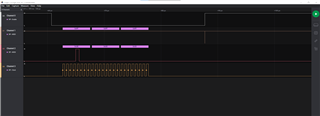
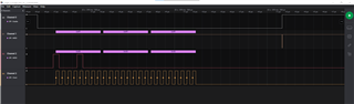
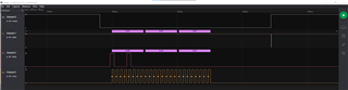
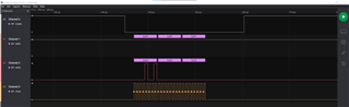
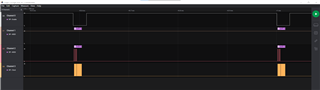
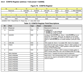
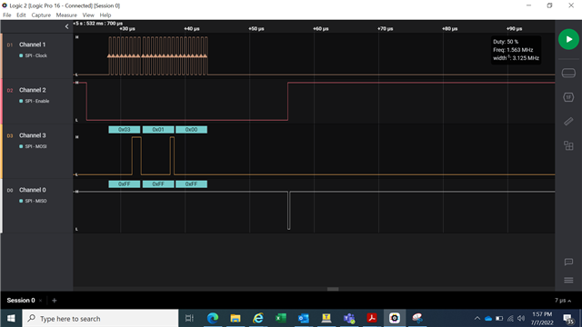
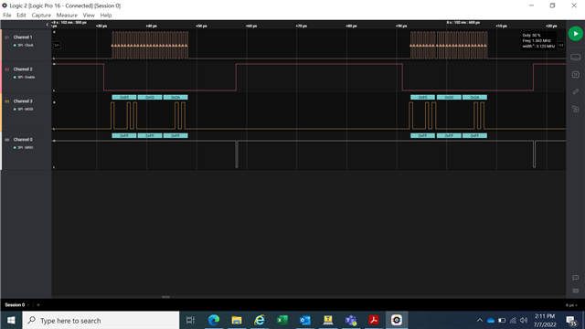
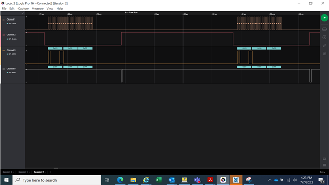
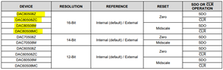
Value read from DAC80508 via SPI is always 0xFF.


Observation:

MOSI: correct output is observed on pin 15(SDI) of  DAC80508.

MISO: output observed is always 0xFF on pin 14(SDO) of DAC80508.

SCLK: Clock is observed.

nCS: Chip select is observed.
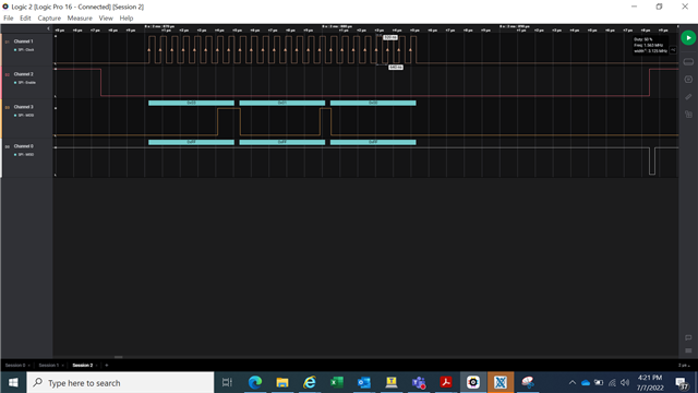
Voltage level:

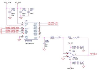
Pin 1(REF): Between 2 & 3 volts

Pin 16(VIO): Between 3 & 4 Volts.

 Attaching data captured on logic analyzer Saleae.

  • Continuation to trailing email/message

    We are using DAC80508 on our custom board as shown below.

    Description of logic analyzer(Saleae) screen shot images in trailing email

    1) a) Write value 0x000A to Trigger register(Address 0x05) to perform soft reset.

             Command: 0X05, 0X00, 0X0A

    1) b) Trigger register(Address 0x05) read value 0xFFFFFF.

             Command : 0X85, 0X00, 0X0A, 0X85, 0X00, 0X0A. 

    1) c) Device ID register(Address 0x01) read value 0xFFFFFF.

             Command: 0x81, 0x00 ,0x00, 0x81, 0x00 ,0x00, 

    1) d) Write value of 0x0000 to Config register(Address:0x03) to enable serial interface and drive SDO when CS is low.

             Command: 0x3, 0X00, 0X00

    1) e) Config register(address 0x03) read value 0xFFFF.

             Command: 0X83,0X00, 0X00, 0X83,0X00, 0X00.

    1) f) Gain register(Address 0x04)read value 0xFFFF.

             Command: 0x84, 0x00, 0x00, 0x84, 0x00, 0x00

    1) g) Status Register(Address 0x07)read value 0xFFFF.

             Command: 0x87, 0x00, 0x00, 0x87, 0x00, 0x00

    2) Write value 0x00 to DAC0(Address: 0x08), this expects to see output logic voltage 0 but voltage level of aprrox. 2.5V is observed.

             Command: 0x08, 0x00, 0x00

    3) & 4) DAC0(Address: 0x08) read value 0xFFFF.

             Command: 0x88, 0x00, 0x00, 0x88, 0x00, 0x00

    5) Write value 0x00 to DAC1(Address: 0x09), this expects to see output logic voltage 0 but voltage level of aprrox. 2.5V is observed.

             Command: 0x09, 0x00, 0x00

    6) DAC1(Address: 0x09) read value 0xFFFF.

             Command: 0x89, 0x00, 0x00, 0x89, 0x00, 0x00

    Note 1: When reading data from DAC80508, Test has been performed by varying delay after first 3 byte for read operation.

    "With delay" example: 1 second, 10 microsecond.

    "Without delay(No delay routine call after first 3 byte read operation). Example: send first three byte then send second 3 dummy byte.

    Note 2:  

    Below 2 test are also performed but output remains constant.

    1) Changing DAC0 register value between 0x00 to 0xFF.

    2) Changing DAC1 register value between 0x00 to 0xFF00.

  • Hi Bharat,

    Have you enabled the SDO via the DSDO bit in the config register?

    If it is enabled, you can also try changing the FSDO bit. There could be a mismatch between how your controller is expecting the data and how the DAC SDO pin is shifting the data out.

    Have you confirmed that you are able to write to the DAC? You can try disabling/enabling the internal reference. 

    Best,

    Katlynne Jones 

  • Hi Bharat,

    We replied at the same time. 

    From this response, I gather that you have not been able to set the DAC output either. Is that correct?

    Edit: Meaning that you do not see a change on the output voltage? 

    Best,

    Katlynne Jones

  • Hi Katlynne,

    Thank you for working on my case,


    > Katlynne : Have you enabled the SDO via the DSDO bit in the config register?

    Bharat: Config Register value is set to 0. Which include Bit9(DSDO) & Bit10(FSDO).

                                As shown in the first image/attachment in message-1

                                Explained in second message point { 1) d) }.

    Question: Is there anything wrong with write operation?

    > Katlynne:  Have you confirmed that you are able to write to the DAC? You can try disabling/enabling the internal reference. 

    Bharat: I can see write transaction on Logic Analyzer as shown in previous attachments.

                  Pin 1(REF) output voltage is between 2 & 3 volts. Bit8(REF-PWDWN) of CONFIG register is set to 0, Means internal reference is used.

    Question: By enabling and disabling internal reference. Does it mean setting/clearing Bit8(REF-PWDWN)?

                                If that is the case, What is expected from it? OR in other words what to interpret by setting/clearing REF-PWDWN.

    > Katlynne: Meaning that you do not see a change on the output voltage? 

    Bharat: Yes, Change in output voltage is not observed.

                                 I would like to inform that a soft reset is performed by writing value 0xA to Trigger Register(Address = 0x5).

                                               My understanding:  This will put SYNC Register (address = 0x2) to 0xFF00.

                                                                            The corresponding DAC output is set to update immediately on a CS rising edge.

                                 Question: Could you please tell if I am missing anything?

  • Hi Bharat,

    I'd like to start with confirming that you can write successfully to the DAC. You are correct, writing 0xA to the trigger register will trigger a soft reset, but if you cannot write successfully then you will not be able to trigger the soft reset. The SYNC register will be defaulted to 0xFF00 when the DAC is powered up without needing to issue a software reset. 

    Please try writing to the CONFIG register to power down the internal reference. 

    Write 0x0100 to register 0x3. If this is successful then you will see 0V on the REF pin. When the internal reference is enabled then you should be seeing 2.5V  on the REF pin as you've observed. 

    If it is unsuccessful then there is something wrong with your SPI command. Please send me a scope shot of this write command. The timings could be incorrect, or you may be using the wrong SPI mode. We can debug the problem after you confirm your results. 

    Best,

    Katlynne 

  • Hi Katlynne,

    Thank you for explanation. 

    DAC write was not successful.

                  Write 0x0100 to register 0x3 => REF PIN(1) stay high(~2.5V).

    Please find below screenshot of SPI write & read operation on logic analyzer. 

    Image 1: SPI Write

    Image 2: SPI Read

    Regards

    Bharat Khanna

  • Hi Bharat,

    Thanks for confirming. It looks like the data is being shifted on the falling edge and sampled on the rising edge. The DAC needs the data to be shifted on the rising edge and sampled on the falling edge. Can you adjust your SPI mode to meet those requirements? 

    The clock can idle high or low, so you can can choose

    Clock polarity = 1 and clock phase = 0 or

    Clock polarity = 0 and clock phase = 1

    Best,

    Katlynne Jones

  • Hi Katlynne,

    After making recommended change " SPI Mode 1, CPOL = 0, CPHA = 1"

    SPI write works fine.

                              Write 0x0100 to register 0x3 => REF PIN(1) voltage drop to ~0.5V.

    Image 1: SPI write

    SPI Read still does not work.

    Image 2: SPI Read

    Output0(Pin 2) & Output1(Pin 3): No change. Always ~2.5V when using internal reference.

    Regards

    Bharat Khanna

  • Hi Bharat,

    Great, good that you were able to successfully write. 

    Can you let me know the full part number you are using? 

    Is it the DAC80508xC or DAC80508x. I think you have the M version because it sounds like the outputs are reset to midscale, but I want to double check that you don't have the MC. The MC (or ZC) has a clear pin instead of the SDO pin. 

    Best,

    Katlynne Jones

  • Hi Katlynne,

    We are using  "DAC80508MC".

    Topic 1:

                   1) Initial state of the pin is high(pulled up). This pin is used only for reading from our side. 

                         As per data sheet: "A low value on the CLR pin causes the DAC outputs of those channels configured for clear operation to update their                               registers and output to the reset value: midscale (DACx0508M). Bringing the CLR pin high causes the device to exit clear mode.".

                   2) If you look at SPI read image in previous message. The pin reads low for a very short duration. Is this an issue?

    Topic 2:

                  > Ktlynne : The MC (or ZC) has a clear pin instead of the SDO pin. 

                   1) My understanding is we can not use this pin as as SDO. Is that correct?

    Topic 3:

                  Irrespective of read operation. As SPI write is confirmed and IC boots up in such a setting that writing to address 0x8 to 0xF should reflect change in pin OUT0 to OUT7. As change in voltage is not observed on OUTX pin, is there any specific register setting that is missing?

    Regards

    Bharat Khanna

  • Hi Katlynne

    Thank you for the support.

    ----------------------------------------------------------------------------------------------------------------------------------------------------------

    Summary:

    I would like to inform, below changes made the DAC working.

    1) Setting PIN 14(SDO/CLR) pin always high.

                    In DAC80508MC module, pin 14 is used as CLR pin.

    2) SPI Mode 1, CPOL = 0, CPHA = 1" is required. The DAC does operation on the rising edge of the clock.

    ------------------------------------------------------------------------------------------------------------------------------------------------------------

    Can you please clarify below query?

                  > Ktlynne : The MC (or ZC) has a clear pin instead of the SDO pin. 

                   My understanding is, we can not use this pin as as SDO. Is that correct? if not, what register setting is required to make PIN 14 as SDO?

    Regards

    Bharat Khanna