This thread has been locked.

If you have a related question, please click the "Ask a related question" button in the top right corner. The newly created question will be automatically linked to this question.

ADC3683EVM: The input frequency range of ADC3683EVM

Part Number: ADC3683EVM
Other Parts Discussed in Thread: ADC3683

Hello, I have to questions about the ADC3683EVM:

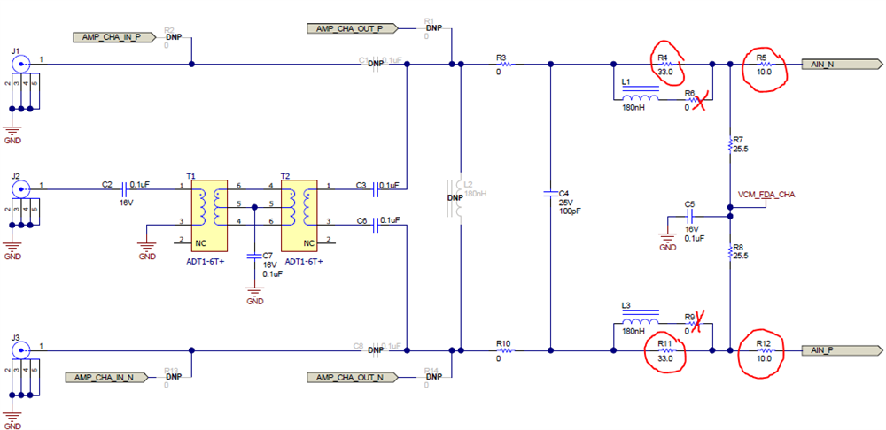
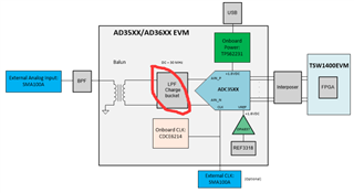
(1) According to the datasheet of ADC3683, the analog input BW is 900 MHz. However, according to the user guide of ADC3683EVM, there is a LPF charge bucket acted as a LPF before the ADC3683. Obviously, the LPF will degrade the analog input BW of the EVM. How can I bypass the LPF charge bucket when I use the EVM?

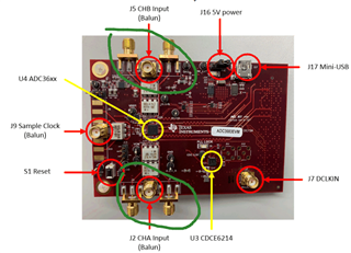
(2) I notice that there are three connectors for the input analog signals (J2 and J5) in the ADC3683EVM, what's the difference between them? Are all of the three connectors connected with the LPF charge bucket?

  • Hello Jingzhan,

    Yes, it is possible to bypass the lowpass filter. To bypass the 30MHz filter, you will need to modify the hardware by placing 0ohm resistors in the filters place. See my image below showing the necessary modifications for channel A. Firstly, R6 and R9 will need to be removed to remove the inductor from the input path. Then, R4, R5, R11, R12 will need to be changed to 0 ohm resistors. This will remove the lowpass filter.

    Regarding your second question, the vertical SMA connectors (J2, J5) are the inputs for driving the ADC single ended. The side connectors are for driving the ADC differentially. In the above image, J1 and J3 are disconnected from the ADC by default since the capacitors C1 and C8 are marked as DNI.

    Regards, Chase

  • Thank you! I understand now.