This thread has been locked.

If you have a related question, please click the "Ask a related question" button in the top right corner. The newly created question will be automatically linked to this question.

ADS7828: ADS7828 doubts

Part Number: ADS7828

Hi.

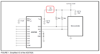
Regarding ADS7828 that is an 8-channel ADC with I2C interface.

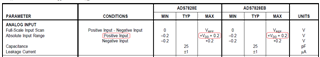
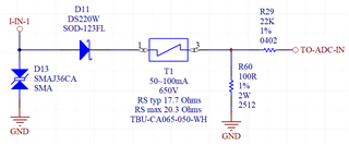
If in the schematic I'm going to have 8x 0/4~20mA current inputs using 8x the circuit below, where a 20mA output from sensors do generate 2V at the 100R sampling resistor. From this resistor to the ADC input there is (currently) a 22K current limiting resistor that I wanted to reduce the value due to the analog input leakage, because I'm considering that in the worst case of transient at input "I-IN-1", it could be generated a voltage spike of 65V max over the 100R resistor during some microseconds. I suppose that there exist internally to ADS7828 analog pins a clamping diode to a positive rail (yes/no?). My question is if that rail is the VCC pin or the VREF voltage. And if I could know what is the maximum current (estimated) that can flow through the internal diode, if it does exist. Initially I plan to use the internal 2.5V voltage reference.

EDIT: The TBU device can take a maximum of 1us to actuate, according to the datasheet.

Regards,
Jeferson.

  • Hi Jeferson,

    There is internal ESD protection and there should be diodes going to VDD and GND. However, this structure is meant for ESD events so it is critical to ensure that the device is not being operated in a state where the maximum input voltage specifications is being violated. It seems like this is the case but I just wanted to emphasize. As for the input current, I believe we typically recommend no more than 10mA to the inputs as that is what the internal diodes are rated for. Ideally, the current should be kept at < 10mA. 

    Regards,

    Aaron Estrada

  • Hi Aaron.
    Thanks very much.

    Considering a maximum peak voltage of 65V at the 100R sampling resistor, series resistor of 10K, and even if I disconsider the voltage drop of internal ESD diode from analog pin to +VDD and also the +VDD voltage itself, that would be 3.3V in my case:
    - 65V/10K = 6.5mA (<10mA)

    The datasheet shows this schematic, with that 5 Ohms series resistor on +VDD pin:

    I would use it like this:

    Do you see any problem?

    The datasheet shows as the picture below. Max voltage at positive input would be +VDD+0.2, I'm not sure if that +0.2V (Vin < +VDD+0.2) would guaranteed by the voltage drop on the internal ESD diode from analog pin to VDD. Or if maybe I would need to add one external diode per analog input, this would complicate things because 0.2V is very small voltage and the board is space-constrained.

    Regards.

  • Hi Jeferson,

    That +0.2V addition comes from the internal ESD diode itself. An analog input > VDD +0.2V will forward bias the internal ESD diode and that is where the 10mA current limit I mentioned above comes from. I think ideally, it would be best to add protection on every analog input pin to be extra cautious but if you can limit the current, I think that will be fine. 

    Regards,

    Aaron Estrada

  • Hi Aaron.

    With ADS7828, if using the internal 2.5V voltage reference and supplying it with 3.3V, is there any problem if the analog input reach also 3.3V? but never surpass 3.3V? That is, Vin_channel = Vsupply = 3.3V and VREF = 2.5V?

    Regards.

  • Hi Jeferson,

    No problem there! The ADC will saturate with an analog input >2.5V but there is no risk for damage. Sustained use of Vin_channel > Vsupply + 0.3V will cause some concern for damage. 

    Regards,

    Aaron Estrada