This thread has been locked.

If you have a related question, please click the "Ask a related question" button in the top right corner. The newly created question will be automatically linked to this question.

ADS1258-EP: Offset at MUXOUTN, AINx and Digital Pin Level Problem

Part Number: ADS1258-EP
Other Parts Discussed in Thread: ADS1258

Hello Sir,

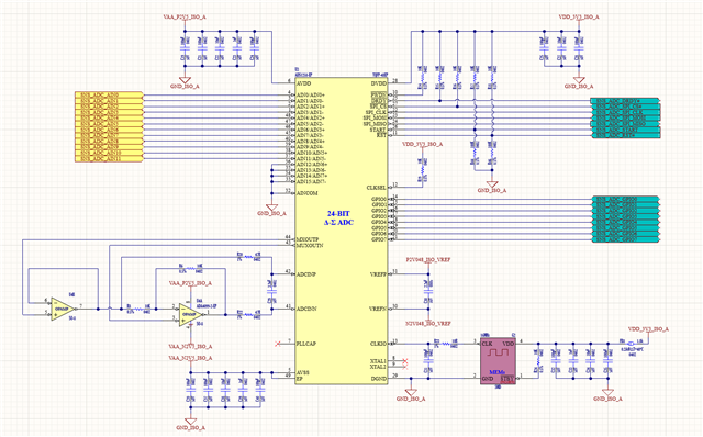
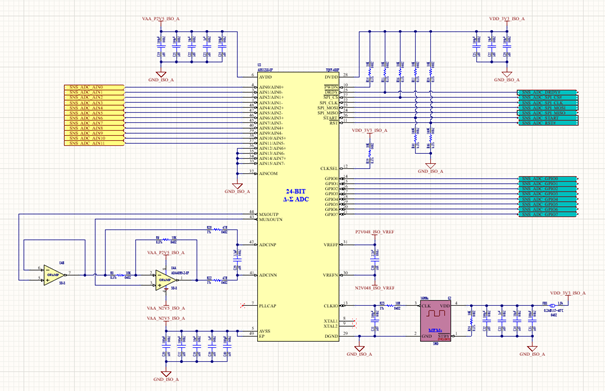
We use ADS1258 as single ended mode, all GPIO as output. Start and reset has 2 option. We use pulled up. Schematic is attached. Register configurstion is as follows.

CONFIG0_DEFAULT = 0x0A; // | CONFIG0_BYPAS_MASK;

CONFIG1_DEFAULT = 0xF0;

MUXSCH_DEFAULT = 0x00;

MUXDIF_DEFAULT = 0x00;

MUXSG0_DEFAULT = 0x08;

MUXSG1_DEFAULT = 0x00;

SYSRED_DEFAULT = 0x00;

GPIOC_DEFAULT = 0x00;

GPIOD_DEFAULT = 0x00;

I can measure AIN3 with above configuration. Also I can see CONFIG0_BYPAS effect as I expect. But I measure some offset voltages.

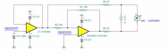
Muxoutn is always 267mV. It does not matter whether CONFIG0_BYPAS register is set or not.

AIN3 measurement is 244,65mV if 253mV is applied. -251,90mV measured if -253mV is applied.

AIN12 is 8,79mV by adjusting MUXSGx registers.

AIN13 is 10,39mV by adjusting MUXSGx registers.

AIN14 is 12,02mV by adjusting MUXSGx registers.

AIN15 is 12,57mV by adjusting MUXSGx registers.

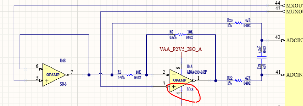
We also detach U4, R20 and R22. But problem continues.

Could you explain why I could not see AINCOM voltage at MUXOUTN?


We supply DVDD with 3.3V. When the start pin low, I can measure 3.3V via multimeter. But when the start pin high, this voltage goes to 3.5V. Then I detach the start pin pull up to measure adc digital pinout. When the start pin low, adc start pin goes 4mV. But when the start pin high, this voltage goes to 4.44V.


Thanks in advance.

Murat

  • I hope this screenshot is better.

  • Hi Murat,

    Thank you for the additional screenshot, this is indeed better

    Have you confirmed that the offset error is not from the signal source itself? What are you measuring?

    Have you tried applying a clean signal, either from a precision source (DP8200) or a low noise voltage reference, and seeing if the ADC can measure this correctly? This is always the first thing you should try.

    Also, can you help explain what is meant by this:

    AIN12 is 8,79mV by adjusting MUXSGx registers.

    AIN13 is 10,39mV by adjusting MUXSGx registers.

    AIN14 is 12,02mV by adjusting MUXSGx registers.

    Is there 8.79mV of voltage on AIN12? Is that what you measure, or is that what you apply? I am not really sure I understand what you are trying to say here.

    Also, it looks like you have START and RESET tied to mid-supply (DVDD) through a pull up and pull down resistor. I would recommend just having a pull-up resistor to make sure the ADC starts up in a known state.

    For the DVDD issue: these measurements are being made between VDD_3V3_ISO_A and GND_ISO_A, correct? And the voltage at DVDD changes when you remove the pull-up on START? Do you have stable power supplies for the ADC?

    -Bryan

  • Dear Bryan,


    - About clean signal source we have tested channel “AIN3” (as a sample channel) by LT6654 precise voltage ref by applying 1V024 but the problem still available in “MUXOUTN”, we measured nearly 267mV instead of 0V.

    - It seems that the problem is internal to ADC because we got the same results on MUXOUTn pin while testing the circuit even without U4 precise opamp (normally connected between MUXOUTx and ADCINx pins)

    - As it is seen from schematic screenshot, AIN12 to AIN15 inputs are all grounded but in ADC readout these channels are nearly ~10mV. So, yes there is 8.79mV of voltage on AIN12.

    - Our circuit has 2 option for start and reset pins. We use just pull up option. We manage start and reset by microcontroller using SNS_ADC_START, SNS_ADC_RESET lines. So there is no mid-supply on start and reset.

    - Yes, measurements were made between VDD_3V3_ISO_A and GND_ISO_A. The voltage at DVDD changes when we manage START pin level (to 0) via SNS_ADC_START. We can supply adc directly by GWINSTEK GPP-4323 power supply or our power circuit that has LT3091, LT3042 LDO's.

    I will do some tests according to your previous answer.

    I hope everything is clear for you. But if it is not clear please let me know.

    Thanks in advance.

  • Dear Bryan,

    For DVDD, the problem is the high level of the adc digital lines that managed by microcontroller. Level of these signals were 5V. Now DVDD problem is solved.  But other problems continue.

    Thanks in advance.

    Murat

  • Hi Murat,

    So I understand correctly: when you put the ADC in auto-scan mode, select AIN12 as the channel (for example) using the MUXSGx register, and then take a measurement, the ADC output reads a value of 8.79mV - is that correct? And this is despite the fact that AIN12 is being measured against AINCOM, and both AINCOM and AIN12 are tied to the same potential (GND_ISO_A)?

    Does this also occur if you bypass the externally signal conditioning circuitry and directly connect MUXOUT to ADCIN (i.e. setting BYPAS = 0)?

    When you input the 1.024V from the LTC VREF, what does the ADC measure? You said that you see 267mV on MUXOUTN, but is that the result from the ADC or are you measuring that voltage using a DMM? And does the measured ADC voltage change when you bypass the signal conditioning circuitry i.e. set BYPAS = 0)?

    Can you provide the voltage reference circuit and the power circuitry as well? It would be good to see how the +/-2.5 V for the ADC/amp is created.

    Finally, I noticed on the schematic that there appears to be a ground symbol connected to the (-Vs) pin on the amplifier. I assume this is just an artifact in the image and is not actually there on the schematic, but just wanted to confirm.

    -Bryan

  • Hi Bryan,

    AINCOM and AIN12,AIN13, AIN14, AIN15 are tied to the same potential reference(GND_ISO_A). And the measurements are about 12mV. So the answer is yes.

    Internal or external circuit results are as follows.

    Multimeter Result Bypass 1, ADC Readout Bypass 0, ADC Readout
    0mV -3.40mV -0.9mV
    1024mV 2041.4mV 1025.41mV
    -1029mV -1966.38mV -984.55mV
    2044mV 3906.04mV 1959.76mV
    -2044mV -3927.30mV -1968.23mV

    Bypass 1 ADC readout nearly double of bypass 0 ADC readout. I did not understand why.

    Yes GND symbol is just an artifact in the image.

  • Hi Murat,

    Nothing stands out as obviously wrong, so here are some additional requests and other things to check:

    • When you are reporting the voltages in the previous table, is this one result from the ADC? Or are you taking multiple results and averaging them? It would be helpful to know how you are reading data from the ADC
    • Can you send me the register settings you are using for all of these tests? It would be helpful to know how fast you are sampling
    • Measure the reference voltage at the ADC pins to be sure it is the correct voltage
    • I am not sure the inverting amp at the output of the reference is the best choice. You can in fact just connect the GND pins on the reference to the VAA_N2V5_ISO_A net and then power the reference using the VAA_P2V5_ISO_A net. This provides the reference with 5V, and then you can remove the inverting amplifier entirely from your circuit. You would need to select a 4.096V VREF in this case however. It appears that you can remove some components and test this configuration on your existing board, to see if it makes a difference 
    • Try disconnecting the power supply from the board and using a benchtop supply to power the circuit. See if this has any impact
    • Are there proper decoupling caps on the amplifiers? Are all decoupling caps on all devices placed close to the respective power pins?
    • Have you checked that the clock is outputting a clean signal using an oscilloscope? Is the clock physically close to the ADC on the board, to ensure that the clock trace length is small and does not pass near other sensitive analog/digital traces?
    • The amplifier circuit has a gain of 2, as shown in the simulation below. This is why you are seeing ~2x the input voltage when BYPAS =1

    If you want to take some data (usually 50-100 samples per test) and send them to me, please do so. Just make sure it is clear what ADC settings were used in the test, and please only send the raw hex data from the ADC.

    -Bryan

  • Hi Bryan,

    The problem is solved. Unfortunately, due to some gain error, an overvoltage (3V - 5V) was applied to the input pins. So everything is ok. Thanks for your help.

    Murat

  • Hi Murat,

    Thanks for letting us know what the problem was and that it has been resolved.

    If you have additional questions, please start a new thread and we will support you there.

    -Bryan