This thread has been locked.

If you have a related question, please click the "Ask a related question" button in the top right corner. The newly created question will be automatically linked to this question.

ADC3683EVM: SPI: no response from ADC

Part Number: ADC3683EVM

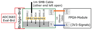
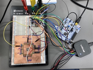
In our development application we need to interface the SPI of the ADC with our FPGA and therefore unsoldered R139, R140, R141, R142 and R144. Then we populated R133, R134, R135, R136 and R137 with 0R resistors to route the SPI lines to the FPGA connector. The adapter PCB from J15 to the samtec high speed connector is plugged in and we manufactured our own breakout board from the samtec connector to SMB and one RJ45 connectors. We use the SMB connectors to interface to our FPGA and the RJ45 connector which is in parallel was left open.

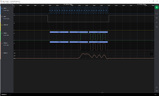
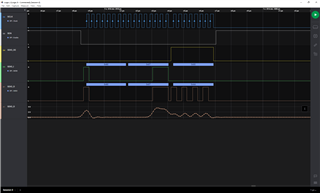
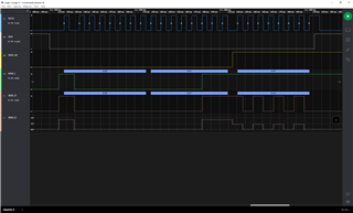
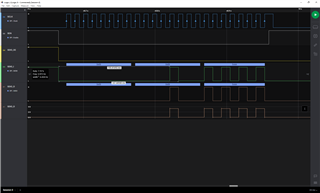
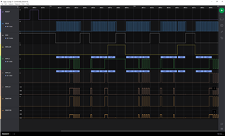
No SPI communication was possible. When probing arround with a scope we noticed that SDIO_O is stuck at the last state of SDIO_I after SDIO_OE switched the bus driver IC to high-z and the adc is not able to drive SDIO_O through the level shifter IC. 

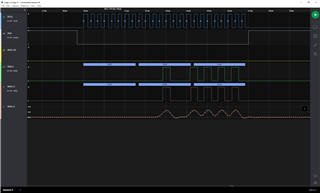
When connecting a normal ethernet cable to the RJ45 connector and leaving the other end open, suddenly SPI works flawlessly. When the SPI signals are instered into the other end of the RJ45 cable and the SMB connectors are left open, the same problem occurs as without the dead end ethernet cable.

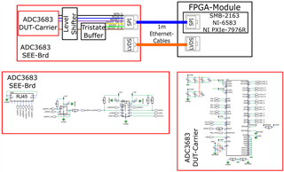
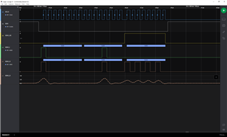
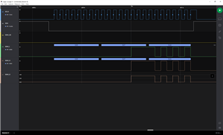
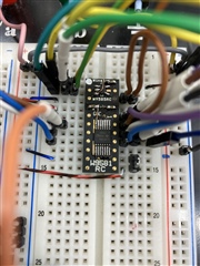
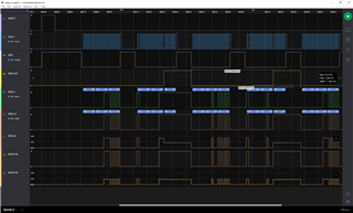
We also experience the same problem when using the ADC on our own development PCB where the SPI signals are routed through the same level shifter and tristate buffer as on the eval board and then routed to an RJ45 connector. Here adding dead end cables or capacitors in the pF range to the SPI wires does not solve the problem.

Any tipps on how to overcome this challenge are welcome!

  • Hi Lukas,

    I am checking into this and will get back to you soon.

    Regards, Amy

  • Hi Lukas,

    Based on the description provided, it sounds like the tri-state buffer is still actively driving its output to whatever the SDOI_I pin is setting, so the ADC is unable to talk back. This situation would only occur if the buffer is still on. The SDIO_OE pin must be high when doing a readback in order to disable the buffer so that the ADC can drive that pin. In summary, the SDIO_OE pin is high when writing from the FPGA to the SDIO pin. SDIO_OE pin is low when reading from the ADC to the FPGA. For readback, SDIO_OE will need to toggle from low to high mid-transaction.

    Regards, Amy

  • Dear Amy,

    thank you very much for looking into our problem.

    Our first guess too was that the tristate buffer doesn't switch correctly and we even soldered a pull up resistor to SDIO_OE as recomended in the tristate buffer's datasheet. I reconstruced the tristate buffer and the level shifter on a breadboard and fed a 3V3 signal into the 3V3 side of the level shifter. On the 1V8 side I looped the signal back to where the tristate buffer's output is connected to on the 3V3 side and everything worked as expected. Only the high level on the 3V3 side was just 1V8 which could be solved by installing a pullup resistor.

    We did some further experiments with the eval board and fed the SPI signals into the RJ45 connector and found out that either an oscilloscope probe or a 1 m SMB cable with an open end has to be connected to SEN in order to get communication working reliably. This fix only works with the eval board though, not with our custom development board. 

  • Hi Lukas,

    Before you modified the board, did you test the SPI interface with the FDTI chip and USB (J17) to confirm that worked? 

    Regards, Amy

  • Dear Amy,

    unfortunately we did not probe arround with the logic analyzer or scope in the original configuration, but we've ordered a second eval board for further debugging

    Best regards,

    Lukas

  • Hi Lukas,

    I'm a bit confused by the experiments that you've tried and the results you see. The SEN line is nominally high due to an internal 21kΩ resistor. Attaching an oscilloscope probe to the line makes sense that it could potentially pull it low (enabling the SPI transaction) however most probes are 1MΩ terminated which is not low enough to overcome the 21kΩ internal pull-up.

    Regarding the open ended cable, this doesn't make sense at all. Leaving the SEN line floating will result in no SPI transactions getting through to the device. Is it possible that in the breadboarded experiment this line was pulled low? This is the only way I can vision the SPI started working.

    What is the IO level of the FPGA? 3.3V? 1.8V? I am wondering if the FPGA IO level is not 3.3V, which means VREF_B on the tristate buffer is not correct, which may potentially be the issue. Is it possible to revert the communication lines back to FTDI for immediate testing? If so, I would recommend doing this.

    Regards, Chase

  • Dear Chase,

    SEN was connected to the FPGA like all the other signal lines via the RJ45 connector and additionally a 1m SMB cable was connected in parallel on SEN. The scope probe was a regular 1:10 testhead and also a 560pF capacitor soldered to the bottom of the SMB connector between SEN and GND made SPI communication with the eval board possible.

    Our FPGA module has a configurable signal voltage and is set to 3V3 (verified by scope measurement and logic analyzer).
    When looking at SEN(3V3), SDIO(3V3), SDIO(1V8), SCLK(3V3) and SDIO_OE(3V3) with the logic analyzer while writing to the ADC no visible difference between with or without the 560pF capacitor/SMB cable/oscilloscope probe can be seen. While reading from the ADC if the correct data value was written to the adress there only is a response if the strange workarround is in place.

    Next week, when I'm back at the office, the new eval board will certainly have been delivered in the meantime so i will try to take a look at those signals and search for any difference. 

    What surprised us more is the fact that we can't get any SPI communication working on our own ADC development board, not even with the 560pF from SEN to GND. Here's the SPI part of the schematic. 

  • Hi Lukas,

    Interesting. Thanks for the extra details, the images you have provided certainly help us understand your setup a bit more. However I do have a few more questions/requests which will further our understanding.

    If possible, can you provide a block diagram of your custom board (only ADC/SPI relevant portions) similar to what you have provided above with the EVM? Can you provide us with a description of the "Bridge-Brd"? Is this the interposer card that is included with the EVM? Is this a custom board, if so, how is SPI being passed through? I'm asking all these questions so we have a solid understanding of your system to discuss internally what could be happening here, because these are strange symptoms which I personally have not encountered.

    Something else you may be able to try once in the lab next week is to swap the 560pF capacitor with a 0Ω resistor, putting the device into a constant read/write state upon the SCLK, just to verify that the SPI transactions begin to function as expected.

    Regards, Chase

  • Hi Chase,

    I will talk to my colleagues on how much of our custom board we can disclose, but the second schematic in my last message already is the whole SPI circuitry of our custom board which also is connected to the FPGA module with a regular ethernet cable like the green adapter board.

    The bridge board is the interposer card that is included with the EVM.

    Thank you very much for looking into our problem!

    I will try out the 0R on SEN as well and try to document everything with the logic analyzer during the process.

    Best regards,

    Lukas

  • Hi Chase,

    attached is the block diagram of our own custom setup. We use a PXI-System with it's FlexRIO FPGA card for SPI and LVDS communication. The output voltage level is set to 3V3 (verified with oscilloscope).


    For debugging I programmed an STM microcontroller on a Nucleo Board to bitbang write and read operations into the adresses 0x07 and 0x08 with data 0xAA.

    The new Eval Board that arrived last week showed sucessful communication with the FTDI chip.

    Then I repopulated the 0R resistors for external communication and connected the SPI signals from the Nucleo board. Now i get a successfull write and read as well. The first eval board, which required the 560pF from SEN to GND to work, is currently with our software developer, so I can't do any probing there right now.

    Unfortunately, our own development board (see block diagram and schematic above), which copies the tristate buffer and level shifter from the eval board, still does not work.

    Do you perhaps have any idea why the second eval board works right away, but the first one and our own board using the same SPI schematic don't? I intentionally use a really low speed on the µC for bitbanging to rule out signal integrity problems.

    Thank you in advance and best regards,

    Lukas

  • Hi Lukas,

    Thanks for the detailed update. So the second EVM is functioning without issue (over both USB and the FMC/external for SPI R/W), that's good, but the first EVM you've tried and your custom board does not work, SPI R/W is still broken. All three solutions have the same exact level shifter (same part, different package) and buffer setup...

    Is the last image in your previous post of the custom board? If so, then the readback is showing 0xFF rather than 0x00 for the data field. The custom board has a 75kΩ pullup resistor on the SDIO line on each side of the level shifter. This would make the part readback 0xFF if the SPI master does not have a much lower input impedance than 75kΩ. Can you remove these pullup resistors?

    Regards, Chase

  • Hi Chase,

    yes, the second EVM works with the change to external, the first one works as well when a 560pF capacitor is soldered from SEN to GND.

    I substituted the SEE-Brd with a breadboard on which just the tristate buffer and the level shifter are inserted (no pull up or pull down resistors) and connected our DUT-Carrier PCB to it (also 1V8 on AVDD and IOVDD, REFBUF with 10k to AVDD, IOGND and GND connected) and the communication still looks like in the last picture from my previous post with 0xFF read from the registers.


    Best regards,
    Lukas

  • Hi Chase,

    I quickly soldered a breadboard together, just the ADC, bypass capacitors, supply voltages, everything needed for SPI and REFBUF with 10k to 1V8.
    Now SDIO_O stays low when reading from the two registers. 


    Best regards,

    Lukas

  • Hi Lukas,

    I spoke to Chase on this and from the picture what I see is a fundamental grounding issue.

    Having a good solid ground between the level shifter and the ADC and level shifter to the driver board is paramount in achieving good signaling.

    I have worked on many designs in the past and have see issues like this before.

    I would recommend soldering a more robust ground between the level shifter board and the ADC copper board you have. A simple wire in this case won't due, even though it is schematically correct.

    Regards,

    Rob

  • Hi Rob,

    thank you! After soldering the tristate buffer and level shifter onto a piece of breadboard stuck onto the groundplane I sucessfully wrote to and read from the "dead-bug" ADC. Unfortunately our real test board still does not work as intended. I'm currently trying to improve grounding as good as possible.

    Best regards,

    Lukas

  • Welcome Lukas!

    Please start a new thread/post if you need anything else.

    Regards,

    Rob