Other Parts Discussed in Thread: AM2434, , DAC8568
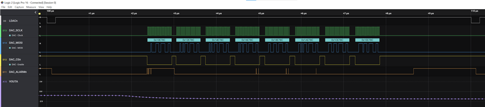
Hi, I am using an AM2434 to program a DAC81416 where LDAC is being independently triggered by an external clock. As soon as LDAC is triggered, I am loading the next set of DAC values ready for the subsequent LDAC.
Question 1:
The LDAC input appears to be level sensitive rather than edge triggered (e.g. not like a DAC8568). What I mean is that if LDAC is held low and I write to a DAC output register, the output changes immediately rather than on the next LDAC falling edge. Is my understanding correct? If so, please clarify in the manual.
This behaviour is not the end of the world but it does mean extra work to manage the LDAC duty cycle.
Question 2:
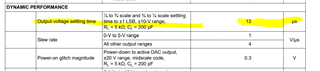
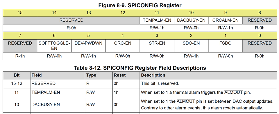
I have read threads here discussing the timing of LDAC to CS (as in it needing to be ~2.4us). I have discovered that I can map the busy bit to the Alarm pin and use the rising edge (i.e. DAC going not-busy) to gate the writing of the next DAC values. Is this an acceptable method?
Question 3:
Do I need to add a delay between writing to the DAC output registers in synchronous mode? I have a natural delay of ~126ns at the moment. It seems to work reliably but should I use the busy bit? My concern is that I will exceed the update time budget.
Incidentally, the sequencing of LDAC is not clear in the manual - a timing diagram would be most helpful.
Thanks,
Steve
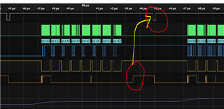
P.S. FYI, I have attached the current timing diagram showing the sequence (ignore the glitches on the Alarm signal - it's a bench rats nest testing the limits of physics). Is there a better way of sequencing this?