This thread has been locked.

If you have a related question, please click the "Ask a related question" button in the top right corner. The newly created question will be automatically linked to this question.

ADC3683: Glitch and input of ADC

Part Number: ADC3683
Other Parts Discussed in Thread: THS4551, , , THS4541

Hi,

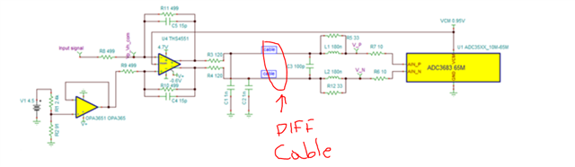
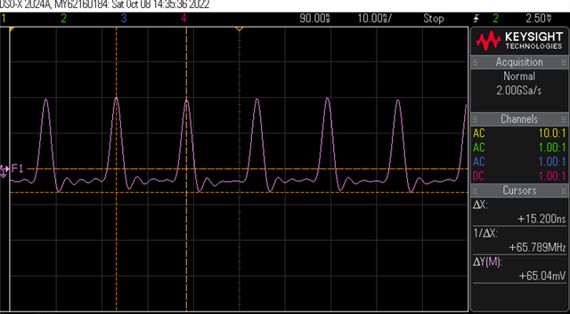
I used THS4551 to drive ADC3683 and found large glitch (200mV peak) on the nodes V_P and V_N.

The waveform is scope calculation result V_P - V_N. The scope bandwidth is 200MHz so the waveform shall be more or less deformed. But according to the frequency it should be the sampling glitch. 

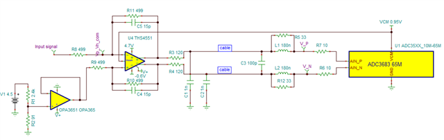
Circuit diagram is shown below, the FDA part is connected to ADC by differential cable around 60cm.

The ADC input filter is designed following the ADC3683 EVM.

Questions:

1. When the driving side is all turned off, the glitch is around 60mV peak. So is the large peak caused by the design at the FDA output?

2. Will it influence the ADC sampling?If so, how to minimize the glitch?

Thanks in advance!

  • Hi Follin,

    Why are you using a 60cm cable between the amp output and ADC input? We would not recommend that. 

    The long cable should be placed before the amplifier. Keep the amplifier input network/filter and ADC close together. This circuit should not be split.

    Also, the THS4145 amplifier is on the ADC3683EVM. Why not use this amplifier?

    Using a long cable could cause a standing wave, which you might see as a glitch. This could cause distortion.

    When the amplifier & signal is turned off there should be no issues. You can verify that by capturing the noise floor of the ADC.

    Regards,

    Rob

  • *** Rob had a typo, the THS4541 is on the EVM, I think you would have figured out, but wanted to add to avoid any unnecessary confusion Slight smile

  • Hi Rob,

    Thanks for your reply. I used the THS4551 mainly because I don't need large bandwidth and it has lower power supply current. Please let me know if there's other major disadvantage compared with THS4541.

    I've captured the noise floor of the ADC. I think the sampling signal doesn't influce the signal.

    But I've watched several channels with only glitch-anti components connnected, the noised floor are different. Some are pretty low around 0.6mVpp, some are 3mVp-p and even one is 12mVp-p. For the larger one, it seems there're pulse in it, but not a normal white noise. 

  • Yes, but still thank you for your remindSlight smile 

  • Hi Follin,

    If you are using your own board design. Would it be possible to send over the FFT noise floor you captured. It would also be good to send the schematics as well.

    Thank you,

    rob

  • Yes, I will uploaded the info later.

  • Ok, thanks Follin. Keep us posted.

    Rob

  • Hi Follin,

    We did a quick measurement on our EVM between the amplifier and ADC. 

    We see the same amplitude level of the glitch, 200mVpp differential.

    In our specific configuration, we see very good performance....however, in our case, the entire circuit is close together and located on the same board with no long cables.

    My only concern with your setup is that you indicated you would have long cables, 60cm, in-between the output of the amplifier to the ADC inputs.

    Unfortunately, we have no way to test this, but the performance might change due to the long lead length in your circuit not the glitch which is inherent to the ADC's internal architecture. 

    Regards,

    Rob