This thread has been locked.

If you have a related question, please click the "Ask a related question" button in the top right corner. The newly created question will be automatically linked to this question.

ADS7028: How to use ZCD module on ADS7028?

Part Number: ADS7028

Hi everyone,

Hope everyone is doing well.

I was working this ADS7028 and encountered several problems.

Most of them are cleared by reading through the following 2 posts. Now I am able to reading the ADC conversion and RMS value.

  1. https://e2e.ti.com/support/data-converters-group/data-converters/f/data-converters-forum/1060295/ads7028-control-ads7028-via-tms320c2000-experiment-kit-piccolo-f28069/3930260#3930260
  2. https://e2e.ti.com/support/data-converters-group/data-converters/f/data-converters-forum/1064651/ads7028-ads7028-zcd-and-rms-setting

However, I am still getting stuck with the ZCD module issue here.

After reading the above 2 posts, I still not getting a clear path that enabling the ZCD module.

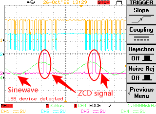
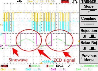
Here is my setup, feed sinewave signal with V_LOW=0.5V and V_HIGH = 2.5V, frequency=60Hz to channel 3, output the ZCD signal on channel 7.

I can verify the RMS value is about 0.711V on channel 3 which very close to my calculation(0.707V) and the voltmeter reading (0.707V).

V_REF is 3.0V.

  1. According to above posts and the attached csv file, the register bit DWC_EN and proper ALERT configuration are required which is not mentioned in the datasheet section 8.3.10?
  2. And Cynthia mentioned "but the ZCD detection would use the RMS value, not the raw input value. " which confused me here, what value did the ZCD detection were using for comparison? Sinewave voltage input or calculated RMS value input?

Could anyone please let me know what is the proper steps to have this completed?

Thank you in advance,

Jinchao

  • I put my steps into a table for your easier understanding. Please let me know if you have any questions or suggestions.

    No Step Description Register Name SPI Data 0 SPI Data 1 SPI Data 2
    1 Reset all registers Write 1b to RST bit in GENERAL_CFG GENERAL_CFG 0x18 0x01 0x01
    2 Send empty message Send empty message 0x00 0x00 0x00
    3 Send empty message Send empty message 0x00 0x00 0x00
    4 Clear BOR flag Clear BOR bit in SYSTEM_STATUS SYSTEM_STATUS 0x18 0x00 0x01
    5 Configure pin Configure only channel 3 as analog input PIN_CFG 0x08 0x05 0xF7
    6 Configure gpio Configure all gpio as digital output, except channel 3 GPIO_CFG 0x08 0x07 0xF7
    7 Configure gpo output Configure all gpo as push-pull output GPO_DRIVE_CFG 0x08 0x09 0xFF
    8 Configure gpo value Configure all gpo to low GPO_VALUE 0x08 0x0B 0x00
    9 Configure ALERT pin Map channel 4 as ALERT output when ALERT is asserted, active low ALERT_PIN_CFG 0x08 0x17 0x40
    10 Configure data Append 4-bit channel ID to output data DATA_CFG 0x08 0x02 0x10
    11 Configure output sample to average Select 64 samples to average OSR_CFG 0x08 0x03 0x06
    12 Stop sequencing Stop sequencing, start sequencing later SEQUENCE_CFG 0x08 0x10 0x00
    13 Select ZCD channel Select channel 3 as ZCD channel CHANNEL_SEL 0x08 0x11 0x30
    14 Configure hysteresis for channel 3 Set the LSB of HIGH_THRESHOLD_CH3 and hysteresis HYSTERESIS_CH3 0x08 0x2C 0x00
    15 Configure high threshold for channel 3 Set the MSB of HIGH_THRESHOLD_CH3 HIGH_TH_CH3 0x08 0x2D 0x7F
    16 Configure ZCD GPO output Select ZCD output (Rising=1, Falling=0) on channel 7 GPO_VALUE_ZCD_CFG_CH4_CH7 0x08 0xE3 0x80
    17 Configure ZCD blanking Configure ZCD blanking time ZCD_BLANKING_CFG 0x08 0x0F 0x00
    18 Configure ZCD output channel Configure channel 7 as ZCD signal output GPO_ZCD_UPDATE_EN 0x08 0xE7 0x80
    19 Enable analog inputs for auto sequencing Enable channel 3 auto sequencing AUTO_SEQ_CH_SEL 0x08 0x12 0x08
    20 Configure sampling rate and mode Set to autonomous mode, high speed, 0000 OPMODE_CFG 0x08 0x04 0x20
    21 Start sequencing Start sequencing, set mode to auto sequencing SEQUENCE_CFG 0x08 0x10 0x11
    22 End of the step
  • Hello, 

    1. According to above posts and the attached csv file, the register bit DWC_EN and proper ALERT configuration are required which is not mentioned in the datasheet section 8.3.10?Thank you for pointing this out. The digital window comparator is needed to be able for the ZDC to function, I will make a note of this to clarify in the datasheet
    2. And Cynthia mentioned "but the ZCD detection would use the RMS value, not the raw input value. " which confused me here, what value did the ZCD detection were using for comparison? Sinewave voltage input or calculated RMS value input?
      This is correct. when using ZDC and RMS on the same channel, then the ZCD will use the RMS output to make the comparison and determine the ZDC output, instead of the voltage inputted at the channel pin. If the voltage at the input is desired to be used for the ZDC then i suggest using a different input channel for ZCD and a different one for RMS. the same input can be connected to two different input channels. 

    Looking through your configuration steps, I believe it should work once you enable the digital window comparator in the GENRAL_CFG register 

    Regards

    Cynthia

  • Thank you Cynthia for your prompt response and we will make changes to our code as you suggested and test it out.

    We appreciate all those detail your provided here which answers a lot of our questions.

    Will keep you posted.

  • Hi Cynthia,

    Yes, enabling the digital window comparator(DWC_EN) in the register GENERAL_CFG will enable the ZCD module to function.

    Below please find my updated table for your reference, just bold the inserted step (step 16) which set the DWC_EN bit in register GENERAL_CFG.

    No Step Description Register Name SPI Data 0 SPI Data 1 SPI Data 2
    1 Reset all registers Write 1b to RST bit in GENERAL_CFG GENERAL_CFG 0x18 0x01 0x01
    2 Send empty message Send empty message 0x00 0x00 0x00
    3 Send empty message Send empty message 0x00 0x00 0x00
    4 Clear BOR flag Clear BOR bit in SYSTEM_STATUS SYSTEM_STATUS 0x18 0x00 0x01
    5 Configure pin Configure only channel 3 as analog input PIN_CFG 0x08 0x05 0xF7
    6 Configure gpio Configure all gpio as digital output, except channel 3 GPIO_CFG 0x08 0x07 0xF7
    7 Configure gpo output Configure all gpo as push-pull output GPO_DRIVE_CFG 0x08 0x09 0xFF
    8 Configure gpo value Configure all gpo to low GPO_VALUE 0x08 0x0B 0x00
    9 Configure ALERT pin Map channel 4 as ALERT output when ALERT is asserted, active low ALERT_PIN_CFG 0x08 0x17 0x40
    10 Configure data Append 4-bit channel ID to output data DATA_CFG 0x08 0x02 0x10
    11 Configure output sample to average Select 64 samples to average OSR_CFG 0x08 0x03 0x06
    12 Stop sequencing Stop sequencing, start sequencing later SEQUENCE_CFG 0x08 0x10 0x00
    13 Select ZCD channel Select channel 3 as ZCD channel CHANNEL_SEL 0x08 0x11 0x30
    14 Configure hysteresis for channel 3 Set the LSB of HIGH_THRESHOLD_CH3 and hysteresis HYSTERESIS_CH3 0x08 0x2C 0x00
    15 Configure high threshold for channel 3 Set the MSB of HIGH_THRESHOLD_CH3 HIGH_TH_CH3 0x08 0x2D 0x7F
    16 Enable digital window comparator Enable digital window comparator module GENERAL_CFG 0x18 0x01 0x10
    17 Configure ZCD GPO output Select ZCD output (Rising=1, Falling=0) on channel 7 GPO_VALUE_ZCD_CFG_CH4_CH7 0x08 0xE3 0x80
    18 Configure ZCD blanking Configure ZCD blanking time ZCD_BLANKING_CFG 0x08 0x0F 0x00
    19 Configure ZCD output channel Configure channel 7 as ZCD signal output GPO_ZCD_UPDATE_EN 0x08 0xE7 0x80
    20 Enable analog inputs for auto sequencing Enable channel 3 auto sequencing AUTO_SEQ_CH_SEL 0x08 0x12 0x08
    21 Configure sampling rate and mode Set to autonomous mode, high speed, 0000 OPMODE_CFG 0x08 0x04 0x20
    22 Start sequencing Start sequencing, set mode to auto sequencing SEQUENCE_CFG 0x08 0x10 0x11
    23 End of the step

    Below please find the screenshots with different high thresholds for channel 3.

    In this way, we can verify the ZCD module on ADS7028 is functioning.

  • I am glad it worked. Please let us know if there is any other questions you may have

    -Cynthia