This thread has been locked.

If you have a related question, please click the "Ask a related question" button in the top right corner. The newly created question will be automatically linked to this question.

ADS4129: sampled output is not proper

Part Number: ADS4129
Other Parts Discussed in Thread: ADS4128, ADS4149

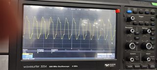
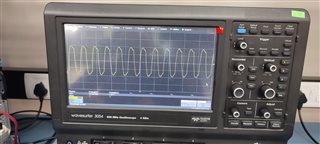
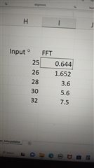
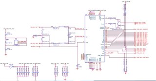
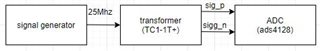
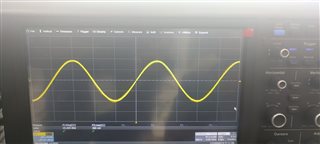
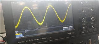
In our custom board we are using ads4129. the register configurations are x"41C0", x"3D80",x"4208", x"DF30", x"0303", x"4A01", x"2503", x"2500". the sampling clock is 24Mhz. we have captured the data on fpga and analyzed in matlab. after aliasing the expected output frequency is not coming. We ensured that the fpga captured output and the adc output(we probed and checked the msb bit of the adc output pins) are matching exactly, so there is no fault. then what might be the reason for this issue? for the reference I have attached the input clk,output_clk, and input fft output for the input frequency.

adc_input_clkadc_output_clkFFT output

  • Vetrivel,

    You are showing address x2503 and x2500. What data value are you using, 03 or 00? 03 is for a test pattern mode.

    Try setting 0x4200 to enable low latency mode.

    Did you try sending a ramp test pattern? This is x250C and x4208. Low latency mode must be disabled to use the test patterns.

    Regards,

    Jim

  • Hi jim, 

    Thanks for the reply. 

    we are configuring toggle pattern (2503) then 64k times we are checking the test pattern. If it it correct then only we are configuring to normal pattern.(2500). Test patterns are coming correctly. The ramp pattern (250C)also coming correctly. 

  • Vetrivel,

    If the test patterns are fine, I would check the analog inputs to the ADC using a differential scope probe. There may be an issue with your analog front end.

    If you would like, send your schematic and we can review it for you.

    Regards,

    Jim

  • Hi jim,

    we are facing a same issue with ads4128 . so I have attached the ads4128 schematic, testing setup, input waveform. the signal generator input signal having more jitter. and the signal power we are giving 0dBm.

  • The register setting are x"41C0", x"3D80",x"4208", x"DF30", x"0303", x"4A01", x"2503", x"2500". the sampling clock is 24Mhz. 

  • Hi Vetrivel,

    Please let us know what signal generator model number you are using?

    Thanks,

    Rob

  • rohde & schwarz SMB 100A

  • for the clear understanding i have attached the ADS4128 schematic.4861.ADC_schematic.pdf

  • Hi Vetrivel,

    Below is your additional information from the other E2E post that I closed out.

    I have the following questions for you:

    Are you using the CMOS output mode or LVDS output mode?

    When you capture the data in the FPGA are you capturing the digital data using offset binary or 2s compliment format?

    Please attach an FFT so we can see what the captured data looks like.

    Also, it might be helpful for us to see more of the schematics? The schematic posted above only shows the ADC.

    Regards,

    Rob

    ***********************************888

    Hi,

    I am using ADS4149 ADC in our custom board. The ADC sampling clock is driven from FPGA.

    Sampling Frequency(Fs) = 24MHz

    ADC input Signal Frequency(Fin) = 328MHz

    ADC input signal power level = -10dBm.

    FPGA Part Number : MPF200T

    I am routing the OCXO clock(24MHz) to ADC through FPGA as Fs. I could see 8MHz at the ADC output.

    Issue 1 Statement :

    Now I am generating the same 24MHz clock by FPGA's internal PLL instead of OCXO and routed to ADC as Fs. Here the ADC output itself not proper. expected is 8MHz but only junks are present.

    I have probed the ADC clock signal by oscilloscope I could make over the following difference between OCXO clock and FPGA's Internal PLL CLOCK.

    OCXO clock is varying from -0.2v to +1.5v with overshoot of 0.4v.(Attachment OCXO_as_ADC_Fs)

    Internal PLL clock is varying from -0.3v to +1.7v with overshoot of 0.5v

    From the ADC datasheet, the clock signal max voltage for LVCMOS single ended configuration is 1.8V. We are using same LVCMOS single ended configuration.

    I can see the internal PLL clock is crossing the 1.8v. Kindly let me know, the issues is happening because of this issue?

    Issue 2:

    The ADC clock is getting coupled in the ADC input signal. Fundamental is 328Mhz. Because of the ADC clock coupling we are seeing the 352MHz, 376MHz and 400MHz @23dB down from fundamental.

    Pls provide suggestion to remove this coupling issue too.