Hi,
I am using ADS4149 ADC in our custom board. The ADC sampling clock is driven from FPGA.
Sampling Frequency(Fs) = 24MHz
ADC input Signal Frequency(Fin) = 328MHz
ADC input signal power level = -10dBm.
FPGA Part Number : MPF200T
I am routing the OCXO clock(24MHz) to ADC through FPGA as Fs. I could see 8MHz at the ADC output.
Issue 1 Statement :
Now I am generating the same 24MHz clock by FPGA's internal PLL instead of OCXO and routed to ADC as Fs. Here the ADC output itself not proper. expected is 8MHz but only junks are present.
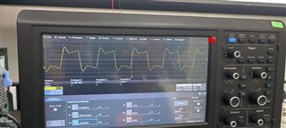
I have probed the ADC clock signal by oscilloscope I could make over the following difference between OCXO clock and FPGA's Internal PLL CLOCK.
OCXO clock is varying from -0.2v to +1.5v with overshoot of 0.4v.(Attachment OCXO_as_ADC_Fs)
Internal PLL clock is varying from -0.3v to +1.7v with overshoot of 0.5v
From the ADC datasheet, the clock signal max voltage for LVCMOS single ended configuration is 1.8V. We are using same LVCMOS single ended configuration.
I can see the internal PLL clock is crossing the 1.8v. Kindly let me know, the issues is happening because of this issue?
Issue 2:
The ADC clock is getting coupled in the ADC input signal. Fundamental is 328Mhz. Because of the ADC clock coupling we are seeing the 352MHz, 376MHz and 400MHz @23dB down from fundamental.
Pls provide suggestion to remove this coupling issue too.
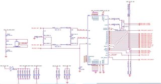
Note: ADC Section Schematic is attached here.